
Application of Al2O3, ZnO, and TiO2 ALD thin films as antireflection coating in the silicon solar cells
- Scientific and Didactic Laboratory of Nanotechnology and Material Technologies, Faculty of Mechanical Engineering, Silesian University of Technology, ul. Towarowa 7, 44-100 Gliwice, Poland
- Department of Engineering Materials and Biomaterials, Faculty of Mechanical Engineering, Silesian University of Technology, ul. Konarskiego 18a, 44-100 Gliwice, Poland
Article Info
Received 21 Jul. 2023
Received in revised form 13 Sep.. 2023
Accepted 15 Sep. 2023
Available on-line 05 Nov. 2023
Keywords: Optical thin film; antireflection coating; atomic layer deposition; solar cells..
Abstract
The article describes the results of a research on the surface morphology and optical properties of Al2O3, ZnO, and TiO2 thin films deposited by atomic layer deposition (ALD) for applications in silicon solar cells. The surface topography and elemental composition were characterised using a scanning electron microscope, and thickness was determined using an optical reflectometer. The samples were structurally examined using a Raman spectrometer. The structural variant was identified: for Al2O3 it is sapphire, for TiO2 it is anatase, and for ZnO it is wurtzite. Possibilities of minimising light reflection using single and double thin film systems below 5% were presented. For the first time, the effectiveness of these thin films on the current-voltage characteristics and electrical parameters of manufactured silicon solar cells was examined and compared. The solar cell with the highest efficiency of converting solar radiation into electricity was obtained for Al2O3/TiO2 and the efficiency of such a photovoltaic device was 18.74%.
Introduction
Optical coatings are widely used in many industries, including optics, optoelectronics, and photovoltaics. Optical coatings can perform various functions. They can be designed to, for example, reduce the reflection of light (antireflection) or, for example, perform the opposite function (reflective). They can also act as a filter and transmit only a specific range of light. They are essential elements for many significant technological usages, such as increasing the conversion performance of solar cells, improving the efficiency of light extraction of diodes, and minimizing lens glare [1–5].
Thin-film antireflection (AR) coatings significantly minimize the light loss in optical components using the transition of light from one medium to another and the dependence of the reflection coefficient on the refractive index. A single quarter-wavelength thin film with a perfect index can exclude reflection at one wavelength and significantly reduce it in a narrow range [4–7]. In order to achieve higher-quality requirements, thin-film AR coatings consisting of different configurations of thin films have been widely applied, such as double thin-film V-type AR, double thin-film W-type AR, multi thin-film AR, and broadband AR. For multi thin-film AR, it is commonly required to deposit a material with a high refractive index for the first thin film (higher than that of the substrate), then deposit a material with a low refractive index for the second thin film (lower than that of the substrate) [3, 5].
One of the important applications of AR is their use in the construction of silicon photovoltaic cells. Silicon is a semiconductor photovoltaic material with a comparatively high refractive index. It is a perfect material for a photovoltaic cell, recently. First, it is non-toxic, and it is also one of the most frequent elements in the Earth’s shell (after oxygen), generating minimal environmental or resource depletion issues if used on a production scale. Silicon photovoltaic cells have drawn significant attention as low-cost and high-performance photovoltaic cells. Pure silicon is a very reflective material. When the light falls on a silicon wafer, it can reflect up to 35% of sunlight. To decrease the amount of sunlight losses, a surface texture treatment is used, and a thin-film AR coating is deposited on a silicon wafer. First, the texture is chemically performed on the plate in order to unfold the surface and multiply the reflection of light from a developed silicon surface. In this way, unfortunately, the negative reflection is not completely eliminated. Therefore, AR coatings are used [3, 5-7].
At present, one of the most commonly used AR thin films in the crystalline silicon photovoltaic cells production are SiO2/TiO2, Si3N4, or SiNx:H [6–9].
In addition to the materials already used, an intensive research is carried out on new materials. One of the promising materials is Al2O3. Although aluminium oxide, a common ceramic material, has been known and used in different fields for centuries, today it makes an active research area in materials science. This is due to the inte-resting properties of Al2O3, e.g., transparency over a wide range of wavelengths, electrical insulation with a band gap over 6 eV, mechanical advantages, and chemical inertness that make it a promising candidate for different high-technology applications. Extensive investigations of this material are currently caused by perspectives of their applications in different electronic structures and photo catalytical and biomedical materials. In photovoltaics, thin films of this material can act as a passivating or anti-reflection layer [3, 6, 8]. Another material that is already known and used in photovoltaics, but rediscovered thanks to advances in deposition technologies, is TiO2. This material has almost ideal properties for use as an AR coating on silicon solar cells. Its refractive index is 2.58. The photoelectrochemical properties of TiO2 are related to the absorption of radiation. The TiO2 is defined by high absorption only in the ultraviolet range. In order to increase the extent of light absorption in the wider range, which is crucial in solar cells and in the degradation of water under the influence of light, the work is ongoing to modify its properties [5, 7]. Due to their electrical properties and transparency, they give the impression of a thin layer made of ZnO. In nature, zinc oxide is an oxidic combination that can be found as mineral zincite that crystallises in a hexagonal structure of wurtzite P63mc. The ZnO belongs to the group of semiconductors. It is characterised by a wide energy gap of 3.37 eV and high transparency. Due to its properties, it can be adapted as an AR coating or a transparent conductive layer (TCL), which are mainly used in electronic devices as display elements, organic diodes, photovoltaic cells, etc. [10, 11].
The choice of deposition method is of great importance in obtaining desired properties for thin films. There are many deposition methods of thin-film AR coatings, such as magnetron sputtering method, vacuum evaporation coating, chemical vapour deposition method, and sol-gel method. The choice of the deposition method is decisive for obtaining a layer with appropriate properties. Chemical vapour deposition is a chemical growth phase in which the reaction takes place in a stream and is called the chemical vapour deposition technology [9–12]. Sputtering is a method of layer deposition which is a type of physical vapour deposition (PVD). In this process, a substrate to be coated with a thin film and a target (source material) are placed into a vacuum chamber that becomes filled with an inert gas (generally, Argon). When the high voltage of electricity is set, positively charged Argon (Ar+) becomes attracted to a negatively charged target material as a cathode and collides with it. Upon the collision, target atoms/molecules are sputtered off and deposited on the substrate, coating it with a layer. Sputtering is conducted in a vacuum to keep the process sterile and free of contamination or impurities. In the vacuum evaporation method, a heated evaporation container with a source material (located in the vacuum chamber) can form a thin film of raw material which leads to the escape of atoms or molecules from the surface gasi-fication and shapes a steam flow that falls on the substrate surface and condenses into a solid thin film [12–18]. In industrial practice, the most used methods are PVD and plasma-enhanced chemical vapour deposition (PECVD). However, they have their limitations. The PVD method covers only the surface of a component perpen-dicular to the stream. In the chemical vapour deposition (CVD) method, it is also possible to cover the surface parallel to the stream. In both cases, the so-called "coat" is obtained. The further away from the stream, the slower the deposition of the layer. Thus, there are variations in thickness.
Within the framework of this article, the use of the atomic layer deposition (ALD) method was indicated. The ALD method is a variety of the CVD method, which is unique in the fact that the precursor and reagent are entered separately into the chamber. They react with each other only on the surface of the coated element. The benefit of ALD is to control the thickness at the molecular level, and uniformly cover the element with developed topography. In addition, the coating produced by this method imitates the shape of the surface, which is often useful, for example, when using a silicon solar cell on a textured surface. Additionally, the possibility of depositing a double layer in one process gives the possibility of using a multi-functional coating. It can play not only the antireflective role but also a passivating one.
The available literature contains reports on the use of an Al2O3 thin film deposited by the ALD method as a passivat-ing layer in thick silicon solar cells and the use of Al2O3, TiO2, and ZnO thin films deposited by the ALD method in thin-film solar cells [19, 20]. However, there is no comparison of the properties of these thin films and their combinations when used as AR coatings in thick silicon solar cells. To the best of our knowledge, there is no reported works on the use of these ALD thin films in a thick silicon solar cell technology and comparing their optical properties on one substrate. In the reported work, the authors compare three different ALDs grown oxide layers such as Al2O3, TiO2, and ZnO, and their possible combi-nations to be used as an AR coating in thick silicon solar cells. In addition, these oxides can act, for example, as a passivating layer or supporting metallic contacts. For the first time, the effectiveness of these layers on the current-voltage characteristics and electrical parameters of manu-factured silicon solar cells was examined and compared.
Material descriptions and research methodology
The aluminium oxide (Al2O3), zinc oxide (ZnO), and titanium oxide (TiO2) thin films and their combinations were deposited using an ALD Picosun R 200 (Espoo, Finland) reactor. The organometallic compounds like trimethyl aluminium (TMA) and diethyl zinc (DEZ) and chloride like titanium tetrachloride were used as a precursor, respectively. In each case, deionized water was used as a reagent. For the selected compounds, the thermal ALD parameters were used with a deposition temperature of 250 °Ϲ with pulse lengths of 0.1 and 4 s creating precursor and water, respectively. The purge step with N2 of 4 s flowing was used between pulses to remove the remains of precursors and reaction by-products. Different sets of the number of cycles of individual thin films were prepared. The number of cycles for single Al2O3, ZnO, and TiO2 thin films was in the range of 100–1000. First, ALD thin films were deposited on a polished silicon substrate (2 × 2 cm plates) with a low roughness coefficient to eliminate the influence of the substrate and characterise it well. Later in the experiment, thin films were deposited on a textured silicon wafer with a P-N junction and with a chemical texture without any passivating or AR layers (5 × 5 cm plates). After the deposition of the tested thin films, metallic contacts were deposited by screen printing.
The surface morphology of the analysed specimens was evaluated by the scanning electron microscope (SEM). The images were taken with a Zeiss Supra 35. The accelerating voltage was 3÷5 kV. To registered images of the surface topography, the secondary electron detector (by the in-lens detector) was used. The qualitative research of chemical elements was also performed using energy-dispersive spectrometry (EDS).
The samples were structurally examined using a Renishaw in Via Reflex Raman spectrometer equipped with a 514.5 nm (green) excitation laser. The spectra were recorded over a wide Raman shift range from 50 to 3100 cm-1. Raman spectroscopy enables the measurement of active Raman phonon modes (in crystalline materials) and active Raman oscillatory modes (in particles). Thanks to this, it is possible to obtain a unique spectral fingerprint of various crystalline polymorphic materials and spectral information from the molecules at the measurement site.
The thickness of the prepared thin films was designated using an FR-pRo-UV/VIS optical reflectometer (Theta-Metrisis SA., Peristeri Greece). The reflected light technique was used for the measurements. Reflectometric measurements are based on the theory of total reflection. This value defines the ratio of reflected light to incident light. A beam of light falling on the sample surface is disturb by reflecting off the upper and lower sides of the thin film. Then, this beam is directed to the CCD matrix by an optical fibre and processed on the computer. In the end, a spectrogram with rectilinear interference oscillations proportional to the thin-film thickness registered on the monitor was obtained. First, the substrate on which natural SiO2 oxides with a thickness of 2 nm were identified was characterised. Their presence in the optical model was considered.
The optical properties of the thin films were determined using a UV/VIS spectrophotometer from Thermo Fisher Scientific Company (Waltham, MA, USA), model Evolution 220. The spectral range of the research was in the range of 300–900 nm. Absolute reflection was determined using an ISA-220 integrating sphere accessory.
Current-voltage characteristics of silicon photovoltaic cells were measured using a solar simulator model SS150AAA. Standard conditions were used in the measurements (Pin = 1000 W/m2, AM1.5G spectrum, T = 25 °C). The most important electrical parameters of the silicon photovoltaic cells were determined by using the I-V curve tracer software.
Results
The microscopic images were registered with a Zeiss Supra 35 using an accelerating voltage of 3÷5 kV. To get images of the surface morphology, the secondary electron (in-lens) detector was used because the specimen and the thin films are very smooth. It was necessary to use high magnification (100 000x and higher) to see surface elements. The surface morphology of the Al2O3, ZnO, and TiO2 thin films was examined. The topography of the thin films prepared by the ALD method is homogeneous and smooth (Fig. 1).
There are no visible discontinuities, cracks, pores or defects. The Al2O3 thin films are characterised by a low-roughness surface topography with repetitive globular structures, like the typical amorphous structure. The ZnO thin film is described by a uniform surface morphology with repeated oval crystallites elongated in the direction of the x-axis. The TiO2 thin film, on the other hand, is characterised by a uniform grain structure. A detailed description of structural studies has been included in previous papers together with discussions on this phenomenon [5, 8, 17, 19]. Electrochemically polished silicon substrates were used in the tests in which the delivery declares the root mean square (RMS) coefficient of roughness below 4 nm. In previous studies, the RMS factor was respectively measured for Al2O3 = 0.28 nm, TiO2 = 2.37 nm, and for ZnO = 1.34 nm by the AFM microscope [21].
The microanalysis of the deposited thin films has been registered with the X-ray EDS. The tests using EDS were aimed at showing that the obtained thin films are homogeneous and free of impurities. Only peaks from elements present in the layer or substrate were recorded. In EDS testing for metallic elements, high voltages from 10 keV are usually used. The lower voltage applies only to light elements. The EDS spectra of thin films of Al2O3, ZnO, and TiO2 are shown in Fig. 2, respectively. In the spectrum of the Al2O3 thin film, peaks of 0.525 and 1.486 keV were recorded, which are from oxygen and aluminium, respectively. Peaks were also recorded for silicon (from the substrate) and for carbon which is always present in the environment. In the spectrum of a ZnO thin film, peaks of 0.525, 1.012, and 8.630 keV were recorded which are from oxygen and zinc, respectively. In the last case, peaks from oxygen and titanium from the thin film and silicon from the substrate were recorded.

In the theoretical group analysis, the representation of alpha-aluminium oxide for optical modes is given as 2A1g + 2A1u + 3A2g + 2A2u + 5Eg + 4Eu. In Raman scattering, vibrations with symmetry A1g and Eg are active. Therefore, seven phonon modes are expected in the Raman shift, at or close to: A1g at 418 and 645 cm-1, and Eg at 379, 431, 450, 578, 750 cm-1. All active modes were registered and shown in Fig. 3(a). In the theoretical group analysis, the titanium dioxide representation has six active Raman modes: 3Eg + 2B1g + A1g. The Eg modes are symmetric stretching of Ti–O bonds. The B1g and A1g are symmetric and antisymmetric bending motions of O–Ti–O, respectively. Their values are at or close to: Eg at 144 cm-1, at 197 cm-1, and at 638 cm-1, B1g at 399 cm-1, and at 513 cm-1, A1g at 519 cm-1. All active modes were registered and shown in Fig. 3(b). In the theoretical group analysis, the representation of zinc oxide is given as 1A1 + 2B1 + 1E1 + 2E2. The optical phonons of ZnO are observed at 327 cm-1, 433 cm-1, and 566 cm-1 which is shown in Fig. 3(c). The peak at 433 cm-1 arises from the first-order Raman scattering by the E2 phonons, which ensures the good ZnO crystal quality. The E2 modes in ZnO of non-polar optical phonons are assigned to the wurtzite structure.

The deposition of single atomic layers in the ALD process is based on two mechanisms: chemisorption on the surface and chemical reactions at the surface of the coated element. Chemisorption should be treated as a chemical reaction between adsorbate molecules (precursor) and atoms of the solid surface (substrate). Therefore, the correct course of the process largely depends on the affinity of the precursor for the substrate and of the reagent for the precursor [22–24]. In the case of Al2O3, during the first step of the ALD cycle, the OH-terminated starting surface is exposed to a pulse of TMA. These precursor molecules will interact with the OH surface groups when binding to the surface, forming CH4 as a reaction product. The CH4 molecules and the rest of TMA are removed from the chamber. The reactant in the case of thermal ALD is H2O. The H2O molecules will remove the remaining CH3 ligands and create CH4 as a reaction product from O-bonds between the Al atoms creating the Al2O3 thin film and terminating the surface with OH-bonds. The remaining H2O molecules and the formed CH4 will be removed during the subsequent pump time, leaving a new OH-terminated surface for the next precursor pulse to react with. It is suggested that the amorphous Al2O3 phase becomes metastable with respect to a crystalline alumina polymorph. Reports in the literature describe the deposits as amorphous, but metastable with respect to a crystalline alumina polymorph [25]. This correlates with the obtained Raman and SEM results.
A similar mechanism occurs in the case of ZnO deposition using diethylzinc (DEZ) and water. The use of this organometallic compound enabled a stable hexagonal crystalline form of ZnO called wurtzite [26] which correlates with the results obtained by the authors. A slightly different situation occurs when a precursor in the form of TiCl4 is used for the TiO2 thin film. The reactant is water, but the growth rate is much lower. It is not clear why the experimentally obtained growth rates of the thin films are up to two times lower than the theoretical value calculated for the process in which no ligands are released from adsorbed TiCl4. It has been discussed that HCl, which is released in the reaction between TiCl4 and surface hydroxyl groups, may re-adsorb and occupy adsorption sites for TiCl4. Nevertheless, this reaction, according to literature data, allows obtaining a stable crystalline structure of anatase TiO2 [27]. The authors confirmed this with Raman studies.
The reflection of light from the samples in the range of 300–900 nm was measured and then their thickness was determined based on these results. Fig. 4 shows a selected experimental and fitted spectrum. All results were distinguished by a high fit factor. The parameter matching R2 was in each case above 0.980 (it should be as close as possible to the value 1). The influence of the number of cycles on the thickness of the deposited thin film is shown in Fig. 5. Based on the obtained results, the growth rate of individual thin films was estimated. Thus, a thin film of Al2O3 grew at 0.1 nm/cycle, ZnO at 0.12 nm/cycle, and TiO2 at 0.036 nm/cycle, respectively.


The Al2O3, ZnO, and TiO2 thin films prepared with a number of cycles from 100 to 1000 were measured. Based on the calculated thicknesses, it was possible to designate the average speed of thin-film growth through one ALD cycle. The aluminium oxide is characterised by approximately 0.1 nm per cycle, for zinc oxide it is 0.12 nm, per cycle and for titanium oxide thin film it is 0.035 nm per cycle. Subsequently, AR coating consisting of two thin films with different thickness and composition was obtained using Al2O3 ZnO, and TiO2 materials.
The possibility of minimizing light reflection was investigated using different materials (Al2O3, ZnO, and TiO2) and their double thin-film combinations (Figs. 6, 7). From the point of view of optical properties, thin films are indeed assumed to be deposited from the lowest refractive index to the highest. Nevertheless, the multifunctionality of the deposited coatings is also considered. As in the SiO2/TiO2 system, although the SiO2 thin film has a lower refractive index, it also acts as a silicon passivating layer, and the Al2O3 thin film can also play such a role. Therefore, the authors decided to deposit such systems, as well.
Single AR coatings allow minimization of light only in a small range. The Al2O3 thin film with a thickness of 90 nm has its minimum reflection in the range of 600– 700 m. Reducing the thickness shifts the minimum to shorter wavelengths [Fig. 6(a)]. Since ZnO has a higher index of refraction than Al2O3 at the same thickness (e.g., 90 nm), the minimum of reflection occurs at longer wavelengths (700–800 nm). As in Al2O3, the tendency of changing the reflection minimum to shorter wavelengths with the reduction of a thin-film thickness is similar [Fig. 6(b)].
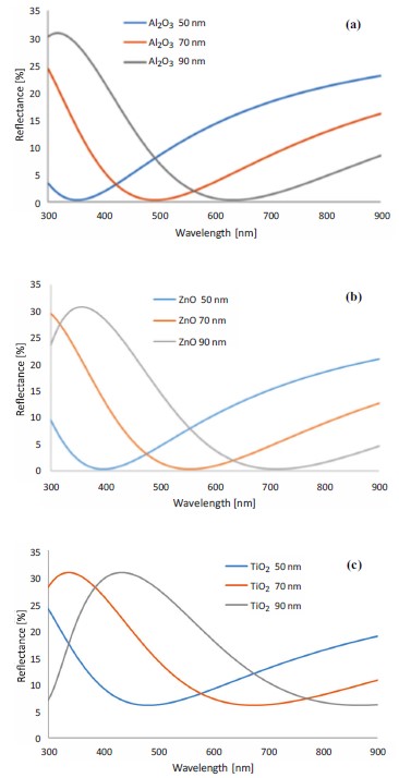
The high refractive index of TiO2 means that to obtain the minimum in the same range as Al2O3 or ZnO, it is enough to deposit a thinner thin film. Nevertheless, the reflection values are slightly higher [Fig. 6(c)]. Fig. 7(a) shows the reflection of light from the surface of silicon covered with thin films of Al2O3, ZnO, and TiO2. The thicknesses were selected to obtain the minimum of light reflection in a similar range. Similar results were obtained for the Al2O3 and ZnO thin films, while for the TiO2 thin film, slightly higher reflectance values were obtained.
Since a single thin film only minimizes reflection in a narrow range, and beyond that, reflection increases significantly. The possibility of minimizing the reflection using a double thin-film AR coating consisting of a combination of Al2O3, ZnO, and TiO2 films was investigated. The best results were obtained for TiO2 27nm/Al2O3 65 nm [Fig. 7(b)]. In the wavelength range of 500–700 nm, the light reflection was below 5%, while in the literature for classic AR coating such as SiO2/TiO2, the reflection was between 8–10% [22] and similar results for Si3N4 [28].

Current-voltage characteristics of silicon photovoltaic cells with selected single and double AR coatings were measured (Fig. 8). On their basis, the electrical parameters of the solar cells were determined (Table 1). The solar cell with the highest efficiency of converting solar radiation into electricity was obtained for Al2O3/TiO2. The performance of such a photovoltaic cell was 18.74%.

Table 1.
Summary of electrical properties of the polycrystalline silicon photovoltaic cells with Al2O3 ZnO and TiO2
thin-film single and double AR coating with different compositions.
Sample |
Isc [mA] |
Uoc [V] |
FF |
η [%] |
ZnO |
632.4 |
953.512 |
0.700 |
16.62 |
Al2O3 |
634.6 |
969.708 |
0.734 |
17.75 |
TiO2 |
637.2 |
975.872 |
0.742 |
18.10 |
Al2O3/ZnO |
638.7 |
957.572 |
0.735 |
17.88 |
Al2O3/TiO2 |
634.6 |
974.037 |
0.770 |
18.74 |
TiO2/Al2O3 |
633.2 |
961.890 |
0.773 |
18.50 |
Conclusions
The article examines the possibility of using metal oxide thin films deposited by the ALD method in the structure of polycrystalline silicon solar cells. For this purpose, the growth rate of the deposited Al2O3, ZnO, and TiO2 thin films was determined. The possibility of minimizing light reflection for different combinations of thin films was investigated. Single thin film made it possible to minimize light reflection in a narrow range. The bigger the refractive index of the thin film, the smaller the thickness needed to obtain minimum light reflection in the same wavelength range. In order to extend the range of minimizing the reflection, double AR thin films were used. The best results were obtained for the combination of thin films with TiO2 and Al2O3 of a thickness of 27 nm and 65 nm, respectively. Then, the electrical properties of the silicon photovoltaic cells with deposited thin films were measured. The solar cell with the highest efficiency (18.74%) was obtained for the Al2O3/TiO2.
Authors’ statement
Research concept and design: M.S.; collection and/or assembly of data: M.S., M.M.S; data analysis and interpretation: M.S., M.M.S.; writing the article: M.S.; critical revision of the article: M.S. and M.M.S.; final approval of article: M.S.
Acknowledgements
Publication supported as part of the Excellence Initiative-Research University program implemented at the Silesian University of Technology in 2023.
References
-
Leon, J. J. D., Hiszpanski, A. M., Bond, T. C. & Kuntz, J. D. Design rules for tailoring antireflection properties of hierarchical optical structures. Adv. Opt. Mater. 5, 1700080 (2017). https://doi.org/10.1002/adom.201700080
-
Mousa, H. M., Shabat, M. M. & Karmoot, M. R. Double layer antireflection coating design for conductive solar cells. Rom. Rep.Phys. 72, 1–18 (2020). https://rrp.nipne.ro/2020/AN72416.pdf
-
Dobrzański, L. A., Szindler, M., Drygała, A. & Szindler, M. M. Silicon solar cells with Al2O3 antireflection coating. Cent. Eur. J.Phys. 12, 666–670 (2014). https://doi.org/10.2478/s11534-014-0500-9
-
Sarkar, S. & Pradhan, S. K. Silica-based antireflection coating by glancing angle deposition. Surf. Eng. 35, 982–985 (2019). https://doi.org/10.1080/02670844.2019.1596578
-
Szindler, M., Szindler, M. M., Boryło, P. & Jung, T. Structure and optical properties of TiO2 thin films deposited by ALD method. Open Phys. 15 1067–1071 (2017). https://doi.org/10.1515/phys-2017-0137
-
Marszalek, M., Winkowski, P. &, Jaglarz, J. Optical properties of the Al2O3/SiO2 and Al2O3/HfO2/SiO2 antireflective coatings. Mater. Sci.-Pol. 32, 80–87 (2014). https://doi.org/10.2478/s13536-013-0156-y
-
Dong, C. et al. Low emissivity double sides antireflection coatings for silicon wafer at infrared region. J. Alloys Compd. 742, 729–735 (2018). https://doi.org/10.1016/j.jallcom.2018.01.384
-
Boryło, P. et. al. Structure and properties of Al2O3 thin films deposited by ALD proces. Vacuum 131, 319–326 (2016). https://doi.org/10.1016/j.vacuum.2016.07.013
-
Jaglarz, J., Pukowska, B., Kisiel A., Olejniczak, J., Mycielski A. & Jurusik, J. Influence of hydrogen treatment of CdTe crystals on the reflectivity spectra. J. Alloys Compd. 371, 125–128 (2004). https://doi.org/10.1016/j.jallcom.2003.08.105
-
Boryło, P. et al. The influence of atomic layer deposition process temperature on ZnO thin film structure. Appl. Surf. Sci. 474, 177– 186 (2019). https://doi.org/10.1016/j.apsusc.2018.03.169
-
Baji, Z. et.al. Highly conductive epitaxial ZnO layers deposited by atomic layer deposition. Thin Solid Films 562, 485–489 (2014). https://doi.org/10.1016/j.tsf.2014.04.047
-
Hou, G. J., Garcia, I. & Rey-Stolle, I. High-low refractive index stacks for broadband antireflection coatings for multijunction solar cells. Sol. Energy 217, 29–39 (2021). https://doi.org/10.1016/j.solener.2021.01.060
-
Sarkın, A. S., Ekren, N. & Saglam, S. A review of anti-reflection and self-cleaning coatings on photovoltaic panels. Sol. Energy 199, 63– 73 (2020). https://doi.org/10.1016/j.solener.2020.01.084
-
Drabczyk, K., Kulesza-Matlak, G. & Drygała, A. Electrolumines- cence imaging for determining the influence of metallization parameters for solar cell metal contacts. Sol. Energy 126, 14–21 (2016). https://doi.org/10.1016/j.solener.2015.12.029
-
Park, H. H. Inorganic materials by atomic layer deposition for perovskite solar cells. Nanomaterials 11, 1–22 (2021).
-
Hossain, A. et al. Atomic layer deposition enabling higher efficiency solar cells: A review. Nano Mater. Sci. 2, 204–209 (2020). https://doi.org/10.1016/j.nanoms.2019.10.001
-
Shanmugam, N., Pugazhendhi, R., Elavarasan, R. M., Kasiviswanatha, P. & Das, N. Anti-reflective coating materials: a holistic review from pv perspective. Energies 13, 1–28 (2020). https://doi.org/10.3390/en13102631
-
Zhang, W. et al. Broadband graded refractive index TiO2/Al2O3/MgF2 multilayer antireflection coating for high efficiency multi-junction solar cell. Sol. Energy 217, 271–279 (2021). https://doi.org/10.1016/j.solener.2021.01.012
-
Schmidt, J. et al. Advances in the surface passivation of silicon solar cells. Energy Proc. 15, 30–39 (2012). https://doi.org/10.1016/j.egypro.2012.02.004
-
Ukoba, O. K. & Jen, T.-C. Review of atomic layer deposition of nanostructured solar cells. J. Phys. Conf. Ser. 1378, 1–14 (2019). https://doi.org/10.1088/1742-6596/1378/4/042060
-
Szindler, M. M., Szindler M., Basiaga M., Łoński, W. & Kaim, P. Application of ALD Thin films on the surface of the surgical scalpel blade. Coatings 11, 1–13 (2021). https://doi.org/10.3390/coatings11091096
-
Hu, Sh.-H., Lin, Y.-Sh., Tseng, T.-K., Su, Sh.-H. & Wu, L.-Ch. Reducing light reflection by processing the surface of silicon solar cells. J. Mater. Sci. Mater. Electron. 31, 7616–7622 (2020). https://doi.org/10.1007/s10854-020-03253-6
-
Leskelä, M. & Ritala M. Atomic layer deposition (ALD): from precursors to thin film structures. Thin Solid Films 409, 138–139 (2002). https://doi.org/10.1016/S0040-6090(02)00117-7
-
George, S. M. Atomic layer deposition: An overview. Chem. Rev.110, 111–131 (2010). https://doi.org/10.1021/cr900056b
-
Prokes, S. M., Katz, M. B. & Twigg, M. E. Growth of crystalline Al2O3 via thermal atomic layer deposition: Nanomaterial phase stabilization. APL Mater. 2, 245–254 (2014). https://doi.org/10.1063/1.4868300
-
Cai, J. et al. A revisit to atomic layer deposition of zinc oxide using diethylzinc and water as precursors. J. Mater. Sci. 5236–5248 (2019). https://doi.org/10.1007/s10853-018-03260-3
-
Aarik, J., Aidla, A., Mändar, H. & Uustare, T. Atomic layer deposition of titanium dioxide from TiCl4 and H2O: investigation of growth mechanism. Appl. Surf. Sci. 172, 148–158 (2001). https://doi.org/10.1016/S0169-4332(00)00842-4