
Interfaces-engineered M-structure for infrared detectors
- Center for Microelectronics and Nanotechnology, Institute of Materials Engineering, University of Rzeszów, al. Rejtana 16, 35-959 Rzeszów, Poland
- International Research Centre MagTop, Institute of Physics, Polish Academy of Sciences, al. Lotników 32/46, 02-668 Warsaw, Poland
- Laboratory for Optical Spectroscopy of Nanostructures, Department of Experimental Physics, Faculty of Fundamental Problems of Technology, Wrocław University of Science and Technology, ul. Wybrzeże Wyspiańskiego 27, 50-370 Wrocław, Poland
Article Info
Received 22 Dec. 2023
Received in revised form 09 Feb. 2024
Accepted 09 Mar. 2024
Available on-line 11 Apr. 2024
Keywords: Molecular beam epitaxy; T2SL; InAs/GaSb/AlSb/GaSb; M-structures; dyspersion relation; numerical calculations.
Abstract
In this paper, the authors report strain-balanced M-structures InAs/GaSb/AlSb/GaSb superlattice growth on GaSb substrates using two kinds of interfaces (IFs): GaAs-like IFs and InSb-like IFs. The in-plane compressive strain of 60-period and 100-period InAs𝑚/GaSb/AlSb𝑛/GaSb with different InAs (𝑚) and AlSb (𝑛) monolayers are investigated. The M-structures InAs/GaSb/AlSb/GaSb represent type II superlattices (T2SL) and at present are under intensive investigation. Many authors showtheoretical and experimental results that such structures can be used as a barrier material for a T2SL InAs/GaSb absorber tuned for long-wave infrared detectors (8 μm–14 μm). Beside that, M-structure can also be used as an active material for short-wave infrared detectors to replace InAs/GaSb which, for this region of infrared, are a big challenge from the point of view of balancing compression stress. The study of InAs/GaSb/AlSb/GaSb superlattice with the minimal strain for GaSb substrate can be obtained by a special procedure of molecular beam epitaxy growth through special shutters sequence to form both IFs. The authors were able to achieve smaller minimal mismatches of the lattice constants compared to literature. The high-resolution X-ray diffraction measurements prove that two types of IFs are proper for balancing the strain in such structures. Additionally, the results of Raman spectroscopy, surface analyses of atomic force microscopy, and differential interference contrast microscopy are also presented. The numerical calculations presented in this paper prove that the presence of IFs significantly changes the energy gap in the case of the investigated M-structures. The theoretical results obtained for one of the investigated structures, for a specially designed structure reveal an extra energy level inside the energy gap. Moreover, photoluminescence results obtained for this structure prove the good quality of the synthesized M-structures, as well as are in a good agreement with theoretical calculations.
Introduction
Nowadays, there has been a significant interest in constructing infrared (IR) detectors due to specific properties of III-V materials, especially for type II superlattices (T2SL) [1–3]. In general, the main issue in IR materials is to achieve new material engineering with appropriate operating parameters. Therefore, a novel approach is the new architecture for T2SL InAs/GaSb structures using an M-type barrier structure.
M-structure InAs/GaSb/AlSb/GaSb superlattice (SL) experimentally proposed by Nguyen et al. in 2007 [4] has been intensively studied. It has a wide range of valence band tunability engineering capabilities [5–7] and the ability to control effective mass via the growth direction [4]. This concept is in a good agreement with theoretical predictions [8]. So far, there are two different areas, where the M-structure can be used: as an absorber material for short-wave infrared (SWIR) radiation and as a barrier material for mid-long and very long-wave IR radiation. In the first case, the M-structure can easily replace the binary T2SL InAs/GaSb. It is very important to emphasize that, in theory, the InAs/GaSb SL is limited and obtaining high-quality materials during the growth process is a technological challenge. The M-structures dedicated to the SWIR region were presented in, e.g., Refs.[7, 9–12]. For the SWIR region, the proper binary InAs/GaSb SL should be about 2/8 monolayers (ML) [13] or 4/8 ML [14]. It has been demonstrated that, assuming InSb-like and GaAs-like interface (IF) thicknesses of no more than 1 ML, it will not be possible to compensate for the stresses between the InAs/GaSb SL requiring an extremely disrupted thickness ratio between the individual layers. The second area where the M-structure is applicable is a T2SL InAs/GaSb SL dedicated to mid-wave infrared (MWIR) [11] and long-wave infrared (LWIR) [15] photodetectors as a barrier material for the holes.
In all cited papers, the main properties of the M-structure were described from the point of view of the applications purpose, e.g., quantum efficiency and dark current density. In this paper, the authors focused on the IFs engineering of M-structures to obtain the best crystallographic structure of the investigated materials. For this purpose, it is necessary to reduce minimal mismatches of the lattice constants to avoid growth defects and dislocations which cause degeneration of the surfaces and significantly degrade the performance of the material. The data obtained for five investigated M-structures are presented. Four of them are dedicated as barrier materials for MWIR and LWIR structures (35E031B1M, 35E032B1M, 35E033B1M, 35E062B1M). The remaining one (sample 35E108B1M) is dedicated as SWIR absorber material [2] – see Table 1. The numerical calculations of the dispersion relations for investigated structures are also presented. They prove the significant impact of IF on the energy gap. The investigation of strain balance is confirmed by the presented high-resolution X-ray diffraction (HRXRD) measurements. The SL was analysed by Raman spectroscopy (results obtained along the growth direction), while the surface analyses were examined by atomic force microscopy (AFM) and Nomarski microscopy. The good quality of such M-structures was also confirmed by theoretical calculations and the obtained photoluminescence spectra (for structure 35E177B1M).
Table 1.
Theoretical assumptions of the investigated M-structure with the number of monolayers (ML) of each component.
Sample no. |
InAs |
GaSb |
AlSb |
GaSb |
Period |
|
(ML) |
(ML) |
(ML) |
(ML) |
|
35E031B1M |
12 |
1 |
5 |
1 |
60 |
35E032B1M |
12 |
1 |
5 |
1 |
60 |
35E033B1M |
11 |
1 |
4 |
1 |
60 |
35E062B1M |
10 |
1 |
6 |
1 |
60 |
35E108B1M |
6 |
1 |
5 |
1 |
100 |
Theory
To study the influence of IFs on the energy gap, the authors calculated the dispersion relation for all investigated M-structures in three different ways.
The nextnano++ software was used to simulation dispersion and band edges diagrams (commercial Schrödinger- Poisson-current solver) [16]. M-structures were simulated as a 6-layer per period (with IFs) and a 4-layer per period (without IFs) with an infinite number of periods in a 1D grid with a spacing of 0.1 nm. For calculating band edges, a classical 8-band kp model was used [17, 18]. A quantum 8-band kp model (with parameters estimated from 6-band kp model) with 16 numbers of electrons and holes along the k-space [010] direction was used to calculate the dispersion diagram. The simulations included strains and lattice constants as a function of temperature, with a simulation temperature set to 300 K for all structures tested. Material parameters taken from the material database included in the nextanano++ software were used for the simulation. Input files for simulation were based on the tutorial [19] and the 1DInAs_InGaSb_SL_k_parallel_k_superlattice_nnp.in nextnano++ sample input file was adopted to the simulated M-structures tested.
In the first approach, the data from Table 1 were used to calculate the dispersion – without IFs. The results are presented in Fig. 1. In the second attempt, the data of the thickness of each ML were taken into account from HRXRD results – see Table 3 – and also without IFs – the results are presented in Fig. 2. And finally, the necessary data for the last approaches shown in Table 3 were taken under consideration with the IFs – the results are presented in Fig. 3.

The horizontal axis in Figs.1–3 represents the wave vector k along SL periodic structure (along x – direction perpendicular to the surface of layers) marked as kSL in the range (−𝜋/𝐿, 0) where 𝐿 is the length of one period of SL, whereas k[010] represents the wave vector k for k-space direction [010] (parallel to the surface of the layers) in the range (0, 0.95) in the unit 1/nm. The vertical axis shows the calculated energy bands in the unit of eV, where the maximum energy of the valence band at k = [0,0,0] was taken as 0 eV for better visualisation and comparison. The energy gap Eg shown in Figs. 1–3 was calculated as difference between the lowest energy level for Γ8 band (electrons states) and the highest energy level for Γ6 band (light holes states) at the Γ-point. Fig. 4 shows the calculated band edges for the conduction band and for heavy holes (HH) and light holes (LH) as a function of position 𝑥 of the M-structures (for the two SL periods). The same figure also shows the probability density functions |𝜓|2 for electrons and holes for the minimum energy level of the conduction band ( Γ8) and the maximum energy level of the valence band ( Γ6), which correspond to the energy levels used to calculate the energy gap 𝐸𝑔 for the dispersion diagrams shown in Figs. 1–3.

It is clearly visible that the IFs significantly change the energy gap for all structures. In Table 2, the energy gaps calculated at Γ-point were collected (the difference between Γ8 and Γ6). The significant differences (compared results from Fig. 2 and Fig. 3) are observed for three M-structures 35E031B1M – over 110 meV; 35E032B1M – over 130 meV, and 35E033B1M – about 130 meV. The differences for the last two M-structures are smaller and equal to about 94 meV for 35E062B1M and 60 meV for 35E108B1M.
Table 2.
Collected E𝑔 at Γ-point (calculated by different Γ8 − Γ6) for M-structures calculated using nextnano++ software. In the column 2, the E𝑔 was obtained using the data from Table 1, in the column 3, the E𝑔 was obtained using the data from Table 3 – without IFs, in the column 4, the E𝑔 was obtained using the data from Table 3 – with IFs.
Sample no. |
E𝑔 (eV) Fig. 1 |
E𝑔 (eV) Fig. 2 |
E𝑔 (eV) Fig. 3 |
35E031B1M |
0.477 |
0.474 |
0.360 |
35E032B1M |
0.477 |
0.471 |
0.341 |
35E033B1M |
0.484 |
0.493 |
0.364 |
35E062B1M |
0.535 |
0.517 |
0.423 |
35E108B1M |
0.676 |
0.668 |
0.608 |
What is also interesting for the last structure, 35E108B1M, the additional energy level appears inside the energy gap [see dotted lines in Fig. 3(e)]. According to the calculation of the wave function, it is assumed that this additional energy level is related to the states assigned to IFs [see Fig. 4(e)] where the probability of the wave functions as a function of x is presented. As can be seen, only for these structures such energy level appears. The authors have not found such additional energy level and such |𝜓|2 shape for any of the energy levels for other investigated structures.

Experiment
Technological processes for the investigated M-structures growth were carried out using molecular beam epitaxy (MBE), by means of a Riber Compact 21T (III-V) system equipped with classical ABN60 dual-zone effusion cells for In, Ga, Al, valved arsenic VAC 500, and antimonic VCOR 300 cracker. In this work, five investigated samples of InAs(𝑚 ML)/GaSb(1 ML)/AlSb(𝑛 ML)/GaSb(1 ML) with different MLs 𝑚 (12, 10, 11, 6 ML) of InAs and 𝑛 of AlSb MLs grown on a GaSb:Te (100) ± 0.5° substrates with a 400 nm GaSb buffer layer were investigated. The temperature of the substrate was measured using the arsenic pyrometer. The following substrate parameters were used during the growth process: rotational speed was 10 rpm, temperature ramp rate was 10 °C/min for the heat-up and 20 °C/min for the cool-down processes, respectively. The removal of oxides from the substrate was carried out by maintaining a temperature of 588 °C for 10 min in a protective atmosphere with Sb and then lowering it to the growth temperature of 530 °C. During 60 min, a GaSb buffer layer with a thickness of 400 nm was deposited at a flux ratio of V/III = 1.57, followed by lowering the substrate temperature down to 473 °C and SL was made. The 60 or 100 repetitions of non-intentionally doped InAs/GaSb/AlSb/GaSb was made with flux ratios of V/III = 1.57, 0.96, 6.54 for GaSb, AlSb, InAs, respectively. After the GaSb/AlSb/GaSb layer sequence, the authors used GaAs-like IFs while InSb-like IFs were used after the InAs layer. An overview schematic of the test samples and the shutter sequence for the SL region, as well as a table with a detailed description of the individual steps are included in Fig. 5.

The HRXRD measurements were performed using a diffractometer with Cu K𝛼1 radiation (𝜆 = 1.540598 Å) by Malvern Panalytical.
The surface morphology was obtained by optical differential interference contrast (DIC) microscopy by Olympus, DSX1000 and atomic force microscopy (AFM) by Brucker Innova.
The authors also present the room temperature Raman spectroscopy spectra for the presented structures. The Raman spectra were obtained using an InVia Micro Raman spectrometer combined with a Leica DM 2500M microscope by Renishaw. The measurements were performed with backscattering geometry and cross-section geometry of samples. The Raman signals were collected by a 50x objective lens, yielding laser spot sizes of about 1 um. The argon laser with a 488 nm wavelength and a 5 mW power was used as an optical excitation source. Exposure time was set as 10 s with 5 scans accumulations.
Photoluminescence measurements were performed using a vacuum Fourier transform spectrometer by Bruker (Vertex 80v) [20, 21]. The setup was equipped with a liquid nitrogen-cooled InSb detector providing high detectivity in the investigated spectral range while the samples were kept in the liquid-helium cooled cryostat connected to the temperature controller which enabled the temperature range of the measurements between 10 and 300 K. The exciting beam was provided with a 660 nm continuous wave laser with a nominal power of 60 mW. The laser line was mechanically modulated at a 800 Hz frequency to provide a reference for filtering the signal via a lock-in amplifier. For power-dependent measurements, the laser beam power was changed with a variable neutral density filter placed in the optical path.
Results and discussion
TheHRXRDmeasurementswere performed for all investigated samples. The authors were able to obtain a high and narrow peak in the 2𝜃–𝜔 scan, recorded around the GaSb (004) reflection, which they assigned to GaSb substrate (see Fig. 6). A detailed view of overlapping zero-order peak with the GaSb substrate is presented in Fig. 6 (f)–(j). Additionally, in all graphs in Fig. 6 (a)–(e), well-resolved sharp high order satellite peaks, indicated by “0”, “±1”, etc. are presented.
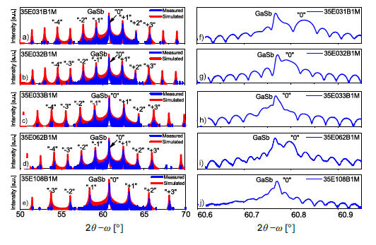
In all cases, Pendelösung fringes were observed around the zero-order SL, as well as around higher order satellite peaks in the 2𝜃–𝜔 scan. All observed satellite peaks are narrow and high, which indicates the high quality of the material. The full width at half maximum (FWHM) of the zero-order SL peak for all samples equals: 76.90 arcsec for 35E031B1M, 88.63 arcsec for 35E032B1M, and 51.66 arcsec for 35E062B1M. Lattice mismatch value was calculated and amounted to −876 ppm, −281 ppm, ≃0 ppm, −457 ppm, and ≃0 ppm for 35E031B1M, 35E032B1M, 35E033B1M, 35E062B1M and 35E108B1M, respectively. Since the lattice mismatch is almost 0 for samples 35E033B1M and 35E108B1M, the FWHM of the zero-order cannot be defined. In addition, based on the simulation of the 2𝜃–𝜔 curve, thicknesses of the InAs, GaSb, and AlSb layers were estimated. Furthermore, matching the measured scans to the theoretical ones allowed the authors to obtain the thickness of the individual IFs: InSb-like, GaSb-like, GaAs-like, and the period of the SL (see Table 3).
Table 3.
The results of the numerical simulation of the HRXRD measurements for investigated samples.

Based on the measurements of the 2𝜃–𝜔 curve, two samples were selected to perform reciprocal space mapping (RSM) measured around symmetric 004. Identical measurement settings were used for both structures: reciprocal lattice points data were collected around the substrate (GaSb) and the sattelite peak "0". Fig. 7(a)–(b) shows the RSM of two structures. For both, the lattice mismatch was impossible to determine, i.e., mismatch was below the resolution of the HRXRD device, which means that the structure of the growing SLs was perfectly matched. Therefore, only one maximum is observed on each of the reciprocal lattice maps. The recorded reciprocal lattice points of the GaSb substrate, as well as zero-order satellite peak exhibited narrowness in both Qx and Qz directions. They are both within the range of −0.00077Å−1 ≤ 𝑄𝑥 ≥ 0.00085Å−1 and −0.0019Å−1 ≤ 𝑄𝑧 ≥ 0.0023Å−1 for 35E033B1M structure; −0.00066Å−1 ≤ 𝑄𝑥 ≥ 0.00095Å−1 and −0.0026Å−1 ≤ 𝑄𝑧 ≥ 0.0019Å−1 for 35E108B1M. The RSM shows a streak perpendicular to the X-axis on the surface of the sample that corresponds to the crystal truncation rod (CTR) along with Pendelösung fringes that are also visible in both cases. Their appearance confirms that the produced structures are of good crystallographic quality. In particular, the streak coming from the analyser is visible (diagonal streak in Fig. 7). Furthermore, the measurements of RSMs, concentrated around reciprocal points of the lattice, unveiled the presence of diffuse scattering (DS). Although a minimal DS signal was noticed, it had no impact on the excellent crystal quality of this structure. The strain balanced studies based on the applied IFs confirmed the presented HRXRD measurements.

The results of AFM and DIC measurements are presented in Fig. 8(a)–(e). All measurements were made with the highest accuracy of 1024 scans per measurement area. The root mean square (RMS) deviation of 3D profile elevations from a 2 μm × 2 μm area performed by AFM is 0.22 nm for 35E033B1M, 0.23 nm for sample 35E031B1M, 0.25 nm for 35E032B1M and 35E062B1M, 0.28 nm for 35E108B1M. These results also show that sample 35E108B1M has the highest RMS roughness value. Nevertheless, all samples indicate excellent surface smoothness, with roughness below 0.3 nm. The lowest RMS value was achieved for sample 35E033B1M. An image of the surface morphology of the investigated structures is shown in Fig. 8(f)–(j). Based on the surface morphology, a shiny, mirror-like surface was obtained for all samples. In case of the samples numbered 35E062B1M and 35E108B1M, the authors were able to detect larger differences. Analysing the images by the comparative method, the largest surface defects can be noticed. The surface with the least number of defects is obtained for samples 35E032B1M and 35E033B1M.

Additionally, results for the Raman spectra of the investigated M-structure samples are shown in Fig. 9. The spectra of SL structures are compared with the spectra of GaSb:Te substrate. The GaSb:Te substrate spectra present two main bands at 227 cm−1 and 236 cm−1, which are attributed to the transverse optical (TO) phonons of GaSb and longitudinal optical (LO) phonons of GaSb, respectively. The weak line at 271 cm−1 is associated with the presence of Te in the material. The spectra of examined InAs/GaSb/AlSb/GaSb SL structures are consistent. The bands characteristics for SL structures are present. The analysis confirmed the presence of Raman modes assigned to each component parts. Most spectral lines have the same position in each of the studied samples, only slight shifts (1 cm−1 – 2 cm−1 ) for some lines were observed. The exact locations of spectral bands are compared in Table 4 and shown in Fig. 9. The InAs-TO mode and InAs-LO mode appear at 217 cm−1 and 236 cm−1, respectively. They both overlap, the first partially, and the second completely with the bands attributed to GaSb vibrations with maximum at 227 cm−1 and 236 cm−1 (GaSb-TO and GaSb-LO vibrations, respectively). The overlapped band at 236 cm−1 is also referred to in the literature as SL LO mode. The observed GaSb-TO and GaSb-LO phonon positions are not shifted with respect to their bulk values. This indicates that the SL crystal structure is well matched.

Additionally, weak InAs second-order phonon modes are also detected in the range from 400 to 500 cm−1. The lines at 318 cm−1 and 338 cm−1 represent AlSb-TO mode and AlSb-LO mode [22, 23]. Raman scattering provides a direct assessment of the IF formed [24]. In all samples of M-structures, bands assigned to specific IFs are recorded. Theweak line at about 185 cm−1 is related to the presence of InSb-like IF. The GaAs-like mode of the second IF is visible as a weak shoulder line at about 244 cm−1 [25, 26] (clearly visible on the spectrum of sample 35E108B1M). The location of the IF band (which is related to the vibrational energy of IF mode) is very sensitive to the local environment. Using the curve fitting method, an analysis of the intensity of individual bands was also performed, which is especially beneficial for overlapping bands. The intensity of bands is presented in Table 4 on a scale: weak, medium, and strong signal. The appearance of bands ranging from 100 cm−1 to 200 cm−1 is considered to show the disorder-activated longitudinal acoustic (DALA) vibrational mode. This effect is related to ionic disorder and interplanar stresses [24]. For sample 35E108B1M, some weak bands were observed in this region (119 cm−1 and 140 cm−1 ), which may indicate some disorders. No distinct bands in other samples could be attributed to well-defined IFs. Furthermore, there was no correlation of IF intermixing and the crystalline quality of the samples is good.
Table 4.
Phonon frequencies of the investigated M-structures.
35E031B1M peak position |
35E032B1M peak position |
35E033B1M peak position |
35E062B1M peak position |
35E108B1M peak position |
Assignment |
cm−1 |
cm−1 |
cm−1 |
cm−1 |
cm−1 |
|
187 (w) |
185 (w) |
186 (w) |
185 (w) |
185 (w) |
InSb-IF |
217 (s) |
217 (s) |
217 (s) |
217 (s) |
217 (s) |
InAs (TO) |
227 (vs) |
227 (s) |
227 (s) |
227 (s) |
228 (s) |
GaSb (TO) |
236 (s) |
236 (s) |
236 (s) |
236 (s) |
236 (s) |
InAs (LO) / GaSb (LO) |
243 (m) |
244 (w) |
244 (m) |
244 (m) |
244 (m) |
GaAs-IF |
318 (w) |
318 (w) |
318 (w) |
318 (m) |
318 (m) |
AlSb (TO) |
338 (m) |
337 (m) |
337 (m) |
337 (m) |
337 (m) |
AlSb (LO) |
The high quality of M-structures was also confirmed for an extra sample numbered as 35E177B1M. In the 2𝜃–𝜔 scan, the authors were also able to obtain a high and narrow peak (assigned to GaSb substrate), as well as well-resolved sharp high-order satellite peaks. FWHM of the zero-order SL peak equals 20.41 arcsec. Lattice mismatch value was calculated and amounted to −260 ppm. In addition, based on the simulation of the 2𝜃–𝜔 curve, thicknesses of the of the individual layers and IFs were estimated (as follows: InAs 1.87 nm, IF InSb-like 0.16 nm, GaSb 0.3 nm, AlSb 1.57 nm, GaSb 0.3 nm, IF GaAs-like 0.10 nm). The 35E177B1M M-structure was taken into account in the numerical calculations of the dispersion relation using nextnano++ software in the same way as M-structures described earlier (from 35E031B1M to 35E108B1M). The results of dispersion with the calculated energy gap E𝑔 were presented in Fig. 10(a) and the probability density function |𝜓|2 with the shape of potentials in Fig. 10(b), analogically to Fig. 3 and Fig. 4.

Photoluminescence from sample 35E177B1M was measured at 10 K to investigate the band gap energy of the structure. The measurements were performed for a range of exciting beam power in order to see the dependence of photoluminescence energy and intensity on the photoinduced carrier density. As is shown in Fig. 11(a), the photoluminescence spectra show a clear signal near the theoretically calculated band gap of 0.705 eV. The signal energy is dependent on the carrier density, as is shown in the inset of Fig. 11(a), which may be related to the band-filling effect where the band edge is partially filled with photoinduced carriers which increases the average energy of the optical transition proportionally to the amount of already occupied states [27]. The parameter 𝛼 [Fig. 11(b)] describing the dependence of the photoluminescence intensity on the excitation power is close to 1, which indicates that the optical transition is mainly a transition with some degree of free-tobound or donor-acceptor pair recombination which lowers the value below 1 [28–30].

Conclusions
In conclusion, the M-structures dedicated for detectors of the IR radiation grown on a GaSb (100) substrate with a GaSb buffer layer with engineered IFs have been investigated for their crystallographic surface morphology and vibrational properties, and energy dispersion.
The special shutter sequences were applied to obtain minimal mismatch lattice constant. For two of the investigated samples, the obtained Δa/a were almost 0, which means that the lattice constant of the M-structures is precisely fitted to the GaSb substrates. For the rest of the investigated samples, the values of the Δa/a below 1000 ppm were obtained, which are the proper values from the point of view of the applications. It is worth emphasizing that the thickness of the sample 35E108B1M is very small compared to the rest, which is important from the point of view of the IF engineering. Whereas for sample 35E033B1M, for which the lattice mismatches were also perfectly fitted, the InSb-like IF was two times bigger. The reason for this is the width of the InAs layers: for sample 35E108B1M, it was equal to 1.88 nm; and for sample 35E033B1M, it was equal to 3.34 nm. It should be emphasized that during all processes the authors were not able to get satisfactory results from the Δa/a with two identical InSb IFs. All presented results were obtained for two different IFs: InSb-like and GaAs-like.
Besides, that presented numerical calculations clearly show that the presence of IFs changes the E𝑔 for each structure and makes it larger than was expected. The same InSb IFs also change the energy gap in the very well-known InAs/GaSb T2SL, but these changes are smaller. Additionally, numerical calculations clearly show that for the special architectures, such as the one shown for the 35E108B1M structure (special means the width of each layer in one period of InAs/GaSb/AlSb/GaSb in relation to the presence of InSb IF), an additional energy level appears inside the energy gap, which, as proved by the calculated |𝜓|2, comes from the IF layers.
The results of photoluminescence are also presented for one of the investigated structures. These results confirm theoretical calculations on relationship between the energy dispersion and the related energy gap, as well as the quality of the synthesized M-structures.
The authors’ study confirms that M-structures are very interesting from the point of view of applications and technology challenges. The results of the present paper, especially the influence of IFs for one of the presented structures, should be interesting with regard to the rapid development of such exciting area of research as IFs states, which in authors’ opinion should be observed experimentally.
Authors’ statement
M.M.: conceptualization of this study, original writing – original draft, analysis of results, writing – review & editing, supervision. D.J.: investigation of MBE growth and methodology. M.R.: XRD formal analysis. A.J.: optical formal analysis. P.K.: investigation of MBE growth. E.B.: AFMformal analysis. M.T.-S.: optical formal analysis measurements. R.W.-N.: Raman spectroscopy measurements, analysis of results. P.Ś.: nextnano++ software calculations and analysis. M.R. and M.M.: photoluminescence measurements, analysis and interpretation.
Acknowledgements
This research was funded by the National Centre for Research and Development (NCBR), under project no. TECHMATSTRATEG-III/0038/2019-00. This research was funded by the Foundation for Polish Science Through the IRA Programme co-financed by EU within SG OP (Grant no. MAB/2017/1).
References
-
Bouschet, M. et al. Temperature dependence study of elec- trical and electro-optical performances of midwave infrared Ga-Free T2SL arrier photodetector. Appl. Sci. 12, 10358 (2022). https://doi.org/10.3390/app122010358
-
Dehzangi, A., Haddadi, A., Chevallier, R., Zhang, Y. & Razeghi, M. Fabrication of 12 pm pixel-pitch 1280 × 1024 extended short wavelength infrared focal plane array using heterojunction type-II superlattice-based pho- todetectors. Semicond. Sci. Technol. 34, 03LT01 (2019). https://doi.org/10.1088/1361-6641/aaf770
-
Müller, R. et al. Advances in type-II superlattice research at Fraunhofer IAF. Opto-Electron. Rev. 31, e144553 (2023). https://doi.org/10.24425/opelre.2023.144553
-
Nguyen, B.-M., Razeghi, M., Nathan, V. & Brown,G. J. Type-II M structure photodiodes: an alterna- tive material design for mid-wave to long wavelength infrared regimes. Proc. SPIE 6479, 64790S (2007). https://doi.org/10.1117/12.711588
-
Lang, X.-L. & Xia, J.-B. Electronic structure and optical properties of InAs/GaSb/AlSb/GaSb su- perlattice. J. Appl. Phys. 113, 043715 (2013). https://doi.org/10.1063/1.4780704
-
Nguyen, B.-M., Hoffman, D., Delaunay, P.-Y., Huang, E. & Razeghia, M. Background limited long wavelength infrared type-II InAs/GaSb superlattice photodiodes oper- ating at 110 K. Appl. Phys. Lett. 93 , 123502 (2008). https://doi.org/10.1063/1.2978330
-
Razeghi, M. & Nguyen, B.-M. Band gap tunability of type II Antimonide-based superlattices. Phys. Procedia 3, 1207– 1212 (2010). https://doi.org/10.1016/j.phpro.2010.01.164.
-
Du, Y., Xu, Y. & Song, G. Theoretical analysis on the energy band properties of N- and M-structure type-II su- perlattices. Superlattices Microstruct. 145, 106590 (2020). https://doi.org/10.1016/j.spmi.2020.106590
-
Razeghi, M. et al. Advances in antimonide-based type-II superlattices for infrared detection and imaging at center for quantum devices. Infrared Phys. Technol. 59, 41–52 (2013). https://doi.org/10.1016/j.infrared.2012.12.008
-
Pour, S. A. et al. High operating temperature midwave in- frared photodiodes and focal plane arrays based on type- II InAs/GaSb superlattices. Appl. Phys. Lett. 98, 143501 (2011). https://doi.org/10.1063/1.3573867
-
Razeghi, M., Dehzangi, A. & Li, J. Multi- band SWIR-MWIR-LWIR type-II superlattice based in- frared photodetector. Results Opt. 2, 100054 (2021). https://doi.org/10.1016/j.rio.2021.100054
-
Hoang, A., Chen, G., Haddadi, A., Abdollahi Pour, S. & Razeghi, M. Demonstration of shortwavelength infrared photodiodes based on type-II InAs/GaSb/AlSb superlattices. Appl. Phys. Lett. 100, 211101 (2012). https://doi.org/10.1063/1.4720094
-
Tang, B. et al. GaAs Based InAs/GaSb superlattice Short Wavelength infrared detectors grown by molecu- lar beam epitaxy. Chin. Phys. Lett. 26, 028102 (2009). https://doi.org/10.1088/0256-307X/26/2/028102
-
Guo, J., Hao, R., Zhao, Q. & Man, S. Band- tailored InAs/GaSb superlattice in infrared appli- cation. Adv. Mat. Res. 750-752, 936–940 (2013). https://doi.org/10.4028/www.scientific.net/AMR.750-752.936
-
Delmas, M., Rossignol, R., Rodriguez, J. & Christol,P. Design of InAs/GaSb superlattice infrared barrier de- tectors. Superlattices Microstruct. 104, 402–414 (2017). https://doi.org/10.1016/j.spmi.2017.03.001
-
Birner, S. et al. Nextnano: general purpose 3-D simula- tions. IEEE Trans. Electron Devices 54, 2137–2142 (2007). https://doi.org/10.1109/TED.2007.90287
-
Birner, S. Modeling of semiconductor nanostructures and semiconductor-electrolyte interfaces. Ph.D. thesis, Univer- sität München (2011).
-
Bahder, T. B. Eight-bandk pmodel of strained zinc- blende crystals. Phys. Rev. B 41, 11992–12001 (1990)https://doi.org/10.1103/PhysRevB.41.11992
-
https://www.nextnano.com/documentation/tools/nextnanoplus/tutorials/1D_superlattice_dispersion_8kp.html
-
Motyka, M. et al. Fourier transformed photoreflectance and photoluminescence of mid infrared gasb-based type II quantum wells. Appl. Phys. Express 2, 126505 (2009). https://doi.org/%2010.1143/APEX.2.126505
-
Rygała, M. et al. Investigating the physics of higher-order optical transitions in InAs/GaSb su- perlattices. Phys. Rev. B 104, 085410 (2021). https://doi.org/10.1103/PhysRevB.104.085410
-
Xu, D. et al. Structure stability of short-period InAs/AlSb superlattices. J. Cryst. Growth 251, 547–550 (2003). https://doi.org/10.1016/S0022-0248(02)02395-3
-
Diaz Reyes, J. et al. Structural and optical charac- terization of type II In0.14Ga 0.86As0.13Sb0.87/GaSb heterostructure doped with zinc grown by liquid phase epitaxy. Vib. Spectrosc. 68, 109–114 (2013). https://doi.org/10.1016/j.vibspec.2013.05.016.
-
Zhang, Y. et al. Molecular beam epitaxial growth of AlSb/InAsSb heterostructures. Appl. Surf. Sci. 313, 479– 483 (2014). https://doi.org/10.1016/j.apsusc.2014.06.009
-
Jasik, A. et al. Strain-balanced InAs/GaSb su- perlattices used for the detection of VLWIR radia- tion. Infrared Phys. Technol. 122, 104109 (2022). https://doi.org/10.1016/j.infrared.2022.104109.
-
Marchewka, M. et al. Strain-balanced InAs/AlSb type-II superlattice structures growth on GaSb substrate by molecular beam epitaxy. Materials 16, 1968 (2023). https://doi.org/10.3390/ma16051968
-
Numai, T. Fundamentals of Semiconductor Lasers, vol. 89–186 (Springer 2015).
-
Schmidt, T., Lischka, K. & Zulehner, W. Excitation- power dependence of the near-band-edge photoluminescence of semiconductors. Phys. Rev. B 45, 8989–8994 (1992). https://doi.org/10.1103/PhysRevB.45.8989
-
Shibata, H. et al. Excitation-power dependence of free exciton photoluminescence of semiconduc- tors. Jpn. J. Appl. Phys. 44, 6113 (2005). https://doi.org/10.1143/JJAP.44.6113
-
Spindler, C., Galvani, T., Wirtz, L., Rey, G. & Siebentritt, S. Excitation-intensity dependence of shal- low and deep-level photoluminescence transitions in semiconductors. J. Appl. Phys. 126, 175703 (2019). https://doi.org/10.1063/1.5095235