ALD-deposited thin films as functional layers in coloured silicon solar cells
Marek Szindler1*
Magdalena M. Szindler2
Julia Popis2
- Scientific and Didactic Laboratory of Nanotechnology and Material Technologies, Faculty of Mechanical Engineering, Silesian University of Technology, ul. Towarowa 7, 44-100 Gliwice, Poland
- Department of Engineering Materials and Biomaterials, Faculty of Mechanical Engineering, Silesian University of Technology, ul. Stanisława Konarskiego 18A, 44-100 Gliwice, Poland
Article Info
Received 15 Jul. 2025
Received in revised form 19 Jan. 2026
Accepted 20 Jan. 2026
Available on-line 09 Mar. 2026
Keywords: surface engineering; thin films; atomic layer deposition; silicon; solar cells.
Abstract
This work explores the use of atomic layer deposited (ALD) ZnO thin films as functional and aesthetic layers in monocrystalline silicon solar cells. ZnO films of varying thickness were deposited on polished silicon wafers and finished solar cells producing distinct interference colours – gold, violet, and green – while enabling precise control over optical properties. Colorimetric analyses in RGB and CIE Lab colour spaces confirmed the tunability of the perceived colour with increasing ZnO thickness. Raman spectroscopy and X-ray fluorescence verified crystalline quality and composition of the ZnO films, while spectroscopic reflectometry demonstrated thickness uniformity and growth rates consistent with ALD characteristics. The deposition of ZnO layers reduced the power conversion efficiency of the solar cells from ~15.2% to ~13.5%, highlighting a trade-off between aesthetics and photovoltaic performance. Nevertheless, the coloured ZnO coatings exhibited potential for integrating photovoltaic modules into architecturally sensitive environments where visual harmony is desired. The results underline the versatility of ALD technology in engineering both the optical and functional properties of solar cells through a controlled thin film deposition.
1. Introduction
Silicon-based photovoltaic (PV) devices dominate the global solar energy market, accounting for over 80% of installations due to their high efficiency, durability, and cost-effectiveness. These solar devices have achieved efficiency levels close to 25%, approaching the theoretical maximum for silicon-based solar cells (the Shockley-Queisser limit). Continuous advancements in material science and manufacturing processes have driven this progress, still solidifying silicon position as the primary material for solar energy conversion [1–4].
One characteristic feature of silicon solar cells is their deep blue colour, which results from optimising their antireflection coating (ARC). This coating minimises light reflection and maximises absorption, thereby enhancing energy conversion efficiency. While this colour is ideal for performance, it limits the aesthetic versatility of solar panels, which increasingly need to blend into diverse architectural environments. For example, heritage buildings under conservation protection require solar installations that respect historical aesthetics. Similarly, modern urban designs often demand customised panel colours to align with specific architectural styles. The requirement for colour customisation introduces technical challenges. Traditional ARC materials like silicon nitride (SiNx) are optimised for blue wavelengths, making deviations from this colour costly in terms of efficiency. Below is a break‑down of colour-specific challenges (Table 1) [4–8].
One promising solution involves a deposition of specified additional thin films, such as zinc oxide (ZnO), onto ready-made silicon solar cells. ZnO is widely recognised for its excellent optical and electrical properties, including high transparency in the visible spectrum and low electrical resistivity. When applied as an ARC or transparent conductive oxide (TCO), ZnO can significantly enhance light absorption through mechanisms such as multiple scattering or reduced surface recombination.
Examples of colour-specific challenges.
| Optical demand |
Application example | Optical challenges |
|---|---|---|
| Red colour | Historic building facades |
High absorption in the red spectrum (λ > 600 nm) |
| Partially transparent |
Glass-integrated solar windows |
Low efficiency (< 15%) due to reduced absorption |
| Light blue colour |
Modern architectural designs |
Conflict with optimal ARC parameters |
Beyond its purely functional role, ZnO thin films have recently attracted increasing attention as colouring and decorative layers in photovoltaic and architectural applications. By precisely controlling film thickness, refractive index, and nanostructure morphology, ZnO-based coatings can generate interference-driven colour effects without pigments, enabling durable, environmentally stable colour customisation of solar panels. Such decorative approaches are particularly relevant for building-integrated photovoltaics (BIPV), where aesthetic integration with façades or heritage architecture is required. However, the available literature addressing ZnO specifically for colouring purposes remains limited compared to its extensive use as a functional ARC or TCO layer, which motivates further investigation in this field. Such decorative approaches are particularly relevant for BIPV, where aesthetic integration with façades or heritage architecture is required. However, the available literature addressing ZnO specifically for colouring purposes remains limited compared to its extensive use as a functional ARC or TCO layer, which motivates further investigation in this field [9–11].
Additionally, doping ZnO with elements like aluminium (AZO) or titanium (TZO) further improves its conductivity and optical performance. Atomic layer deposition (ALD) has appeared as a cutting-edge technique for fabricating ZnO thin films with exceptional precision and uniformity.
It should be emphasised that ZnO may play different roles depending on its position within the layer stack. When employed directly as a functional ARC or TCO layer, ZnO primarily influences charge transport and optical losses. In contrast, when deposited as an additional top coating acting mainly as a colouring layer on an already existing protective or functional coating, its contribution is predominantly optical, with minimal impact on the electrical performance of the device.
ALD enables conformal coating on complex nanostructures, ensuring consistent layer thickness at the atomic scale. This capability is particularly advantageous for applications that require high-aspect-ratio structures, such as nanowire arrays or textured silicon surfaces. Compared to conventional methods like sputtering or chemical vapour deposition (CVD), ALD provides superior control over film composition and morphology, allowing researchers to tailor optical effects to achieve desired colours while maintaining high efficiency (Table 2) [12–15].
Recent studies have demonstrated the potential of ALD-deposited ZnO layers applied directly to finished silicon solar cells. This approach represents a significant
Key differences between ALD, sputtering, and CVD for achieving desired optical effects.
| Parameter | ALD | CVD | Sputtering |
|---|---|---|---|
| Layer uniformity |
± 1% thickness error |
± 5% thickness error |
± 10% thickness error |
| Colour customisation |
High | Moderate | Low |
| Cost per wafer |
$0.50–$0.80 | $0.20–$0.50 | $0.10–$0.30 |
advancement in PV technology by enabling post-manufacture customisation of cell properties. For example [15–18]:
-
enhanced efficiency: ZnO nanorods grown on ALDdeposited AZO seed layers have been shown to increase power conversion efficiency by over 27% compared to cells without these coatings;
-
improved aesthetics: by manipulating layer thickness and refractive indices, researchers can produce a wide range of colours while minimising light reflection to below 5%, ensuring both visual appeal and optimal performance;
-
transparent electrodes: ALD-deposited TZO films have been successfully implemented as top electrodes in nanostructured silicon solar cells, achieving high transmittance (> 80%) in the visible range while maintaining low resistivity.
These innovations highlight the versatility of ALD technology in addressing both functional and aesthetic challenges in PV applications. Through the integration of improved energy conversion performance and enhanced architectural adaptability, the PV sector is progressing toward a future in which solar panels achieve high efficiency while harmoniously blending into their environment [19–23].
2. Materials and research methodology
Fragments measuring 20 × 20 mm2 were prepared from high-purity, mirror-polished silicon wafers – materials typically utilized in electronic applications – by manual scoring with a diamond scribe. ZnO thin films were subsequently deposited using an ALD Picosun R-200 system (Espoo, Finland). Diethyl zinc (DEZ) served as the metal precursor, while deionized water functioned as the oxidizing agent (Fig. 1). Thermal ALD processes were carried out at 250 °C, employing pulse durations of 0.1 s for DEZ and 4 s for water. Each precursor pulse was followed by a 4 s argon purge to eliminate residual reactants and by-products. The total number of ALD cycles varied from 50 to 1000, depending on the target film thickness. Although ZnO deposition was initiated from as few as 50 ALD cycles, the films grown below approximately 250 cycles correspond to the initial nucleation regime of ALD growth. In this early stage, sub-monolayer coverage, island formation, and delayed coalescence may occur, resulting in discontinuous films with non-uniform thickness. Such layers do not produce well-defined optical interference patterns, which limits the accuracy and reliability of thickness determination by spectroscopic reflectometry.
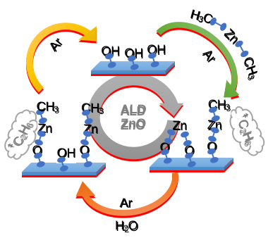
Fig. 1. ALD process: schematic of one cycle of ALD ZnO growth.
Consequently, only ZnO films deposited with 250 or more ALD cycles – where a continuous and optically coherent layer is formed – were considered in the quantitative thickness, colorimetric and optical analyses presented in this work.
Film thickness and visual colouration were evaluated by means of spectroscopic reflectometry using a FR-pRoUV/VIS system (ThetaMetrisis S.A., Peristeri, Greece). Measurements were taken in the reflectance mode. Reflectance spectroscopy serves as the foundational principle for reflectometers. It quantifies the ratio between the acuteness of reflected light waves and that of incident light waves. Typically, the incident light beam is directed onto the sample surface, where it subsequently reflects from both the top and bottom layers, giving rise to interference effects. This reflected beam is then guided through an optical fibre to a CCD matrix, which is connected to a spectrometer via a computer. On the monitor, observers can visualise a spectrogram showcasing linear interference patterns, directly proportional to the thickness of the layers being analysed.
Structural characterisation of the samples was carried out using a Renishaw in Via Reflex Raman spectrometer equipped with a 514.5 nm (green) excitation laser. Spectra were collected across a broad Raman shift range spanning from 50 to 3100 cm-1. Raman spectroscopy enables the detection of Raman-active phonon modes in crystalline materials and vibrational modes in particulate systems. This technique provides a distinct spectral signature for different crystalline polymorphs and enables the extraction of molecular-level information from the probed region.
Complementary analysis of the chemical composition of the deposited thin films was performed using an EDX‑7000 X-ray fluorescence (XRF) spectrometer (SHIMADZU, Kyoto, Japan). XRF is a non-destructive analytical method that relies on the emission of characteristic X-rays from elements upon excitation by incident X-ray radiation of higher energy. The EDX-7000 operates within an energy range corresponding to X-ray wavelengths from approximately 0.31 nm (at 4 kV or 4000 eV) down to 0.025 nm (at 50 kV or 50 000 eV), enabling the detection of elemental signals in the range of 25 to 310 picometers.
Based on the preliminary analysis of layer thickness and optical appearance, the ALD process was subsequently replicated on three monocrystalline silicon solar cells. Deposition was performed with 500, 750, and 1000 ALD cycles, resulting in a gradual, cycle-dependent variation in film colour. The current–voltage (I-V) characteristics of the silicon PV devices were evaluated using a solar simulator (model SS150AAA) under standard test conditions: irradiance of 1000 W/m2, AM1.5G spectral distribution, and a temperature of 25 °C. Key electrical performance parameters of the solar cells were extracted using dedicated I-V curve tracing software.
3. Results and discussion
Figure 2 presents the Raman spectrum of the ALDdeposited ZnO thin film obtained after 900 ALD cycles. The shown spectrum is representative of all fabricated samples, as no significant differences were observed between individual measurements. The Raman spectrum of the ZnO sample exhibits features characteristics of the hexagonal wurtzite structure. The dominant Raman band at 433 cm-1 is assigned to the non-polar E2(high) phonon mode, which is commonly regarded as a fingerprint of well-crystallised ZnO and is widely reported for ZnO thin films and nanostructures [24–26]. Weaker bands observed in the low-frequency region (327–331 cm-1) are attributed to second-order phonon scattering or combination modes, typically associated with nanocrystalline ZnO. A defectrelated band appearing near ~ 531 cm-1 is commonly linked to lattice imperfections such as oxygen vacancies or zinc interstitials [26, 27]. The Raman band at 566 cm-1 corresponds to the longitudinal optical E1(LO) phonon mode, whose intensity is strongly influenced by defect density and carrier concentration. The presence of this mode, together with higher-order Raman features at elevated wavenumbers, suggests structural imperfections typical of nanostructured ZnO thin films [25–27].
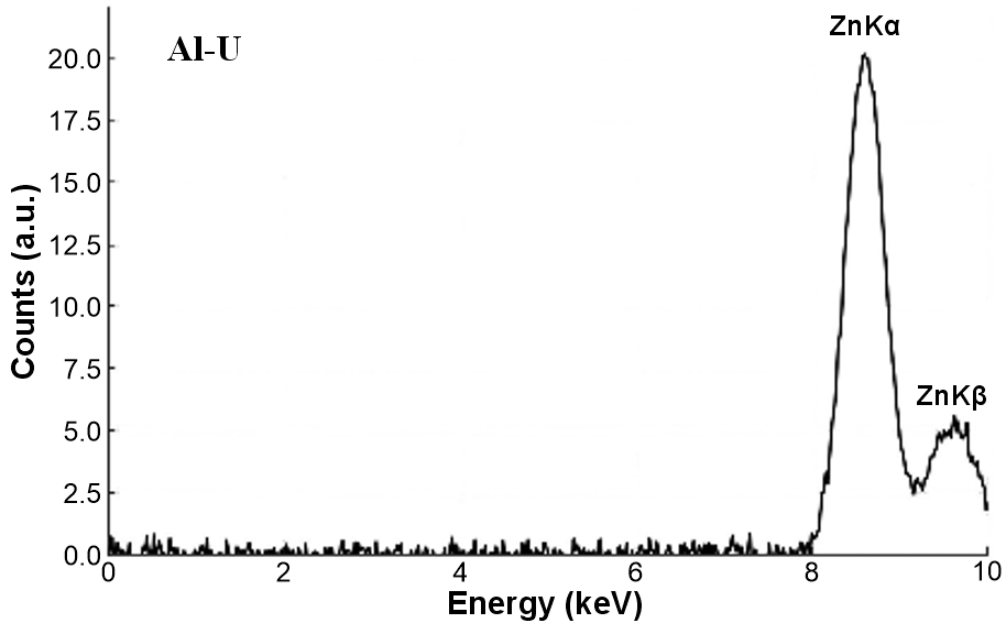
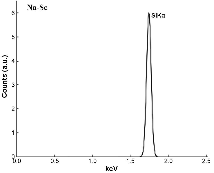
The XRF spectrometry tests confirmed the presence of Zn on the surface of silicon samples. An instance spectrum
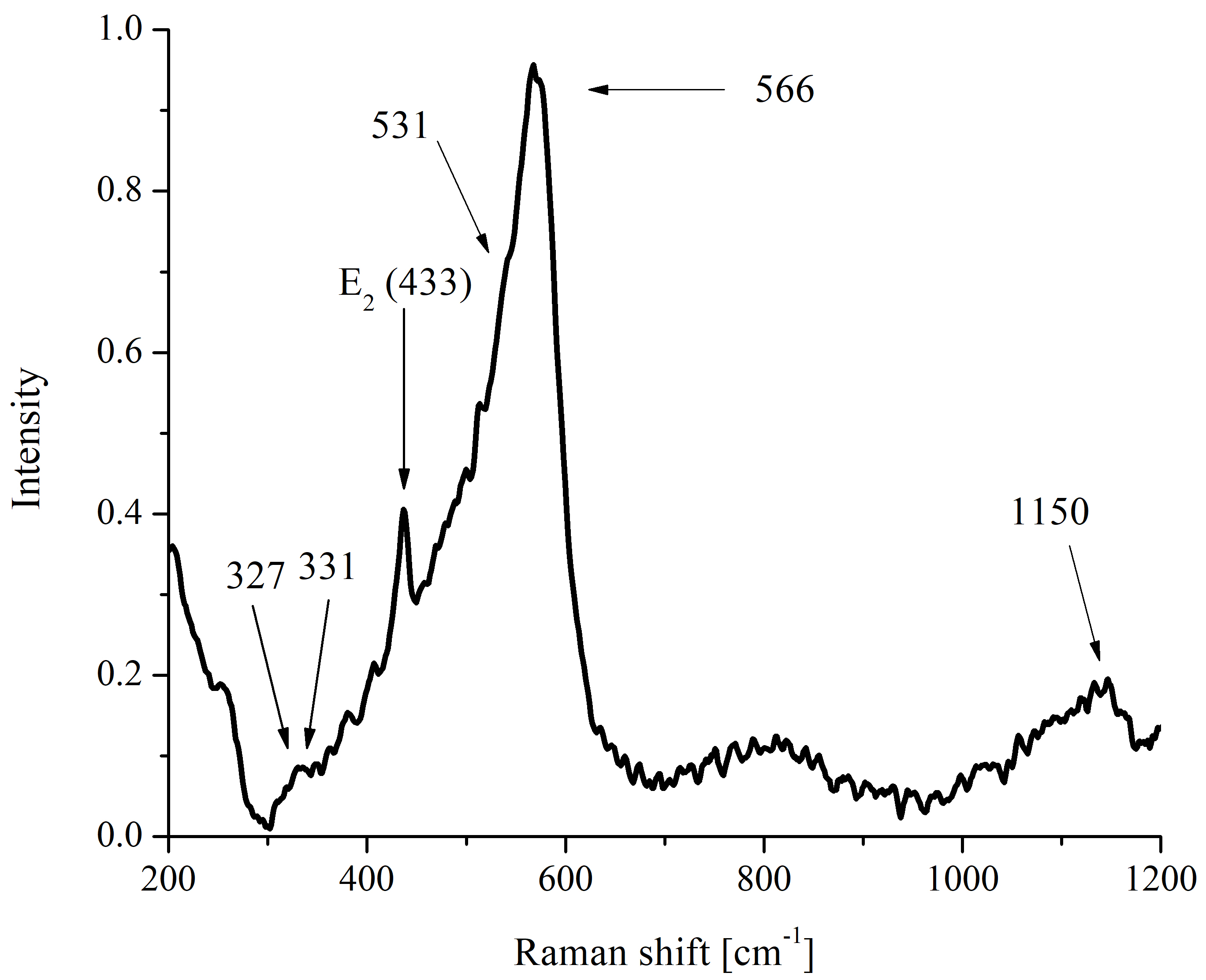
Fig. 2. Raman spectra of ALD ZnO thin film after 900 cycles.
for a silicon sample covered with a ZnO layer after 900 cycles is shown in Fig. 3. During the scan in the Al–Au range, peaks corresponding to Zn were recorded, while during the scan in the Na–Sc range, a peak originating from the silicon substrate was detected. It should be noted that although XRF spectroscopy is well-suited for the detection and qualitative analysis of medium- and high-atomicnumber elements such as Zn, it has significant limitations in detecting light elements, including oxygen. The characteristic X-ray emission lines of oxygen occur at very low energies and are strongly attenuated by air paths and detector windows, resulting in insufficient sensitivity and unreliable quantification. Consequently, the XRF analysis in this work was focused on confirming the presence of Zn in the deposited layers rather than determining the oxygen content. The formation of ZnO was ensured by the selflimiting ALD process employing DEZ and water as precursors and was independently verified by Raman spectroscopy, which confirmed the characteristic phonon modes of crystalline wurtzite ZnO.
(a)
(b)
Fig. 3. Dispersive XRF spectra of Si sample covered with the ZnO layer after 900 cycles.
In this study, a film thickness was employed as the principal variable because all ZnO layers were deposited using identical ALD parameters, including precursor chemistry, substrate temperature, and pulse–purge sequence. Raman spectroscopy confirmed the formation of the wurtzite (hexagonal) ZnO phase for all investigated samples, indicating consistent crystallographic ordering. Wurtzite ZnO is characterised by a well-defined refractive index in the visible spectral range, typically reported to be approximately n ≈ 1.9–2.0, which allows the optical response of the films to be reliably interpreted in terms of thickness-dependent interference effects. Under these deposition conditions, ALD is known to produce highly uniform and conformal films with limited microstructural variation over moderate thickness ranges. While gradual grain coalescence with increasing thickness cannot be entirely ruled out, these effects are expected to be secondary to optical interference, absorption, and interfacerelated phenomena. A detailed quantitative analysis of grain-size evolution would require complementary highresolution microscopy techniques beyond the scope of the present work.
The thickness of the deposited ZnO thin films was determined by spectroscopic reflectance. This technique is based on the analysis of wavelength-dependent interference patterns generated by multiple reflections of incident light at the air/ZnO and ZnO/silicon interfaces. The recorded reflectance spectra were fitted using an optical model that accounts for the ZnO refractive index and the known optical properties of the silicon substrate. Film thickness was extracted by matching the experimental interference fringes with simulated spectra using dedicated analysis software provided with the FR-pRo-UV/VIS system. This non-destructive method enables accurate thickness determination over a wide range of nanometer-scale film thicknesses and was used to establish the thickness–cycle relationship. Figure 4 illustrates the relationship between the number of deposition cycles and the resulting thickness of the ZnO thin films. Based on these measurements, the growth rate for each film was calculated. The growth rate of the ALD ZnO layer ranged from 0.15 to 0.19 nm/cycle. During the initial growth phase, up to approximately 500 cycles, the growth rate of the samples fluctuated between 0.15 and 0.19 nm/cycle. Beyond 500 cycles, the growth rate remained steady at 0.17 nm/cycle.
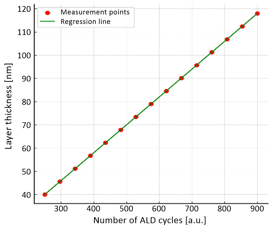
Fig. 4. The influence of the number of ALD cycles on the thickness of the deposited layers.
In conjunction with the thickness measurements of the deposited layers (Fig. 4), comprehensive colorimetric analyses were performed. The study employed advanced software tools capable of determining the colour coordinates within multiple colour spaces, including RGB, HUE, and CIE Lab. The evolution of RGB values as a function of the number of ALD cycles is presented in a two-dimensional format in Fig. 5 and further summarised in Table 3. It is important to note, however, that the RGB colour space does not accurately replicate the full range of colours perceived by the human visual system when observing the examined surfaces. This is primarily due to the inherent limitations of RGB, which lacks perceptual
nm

Fig. 5. The impact of the number of ALD cycles on the colour of the ZnO thin film deposited on a silicon substrate showing in the 2-stage RGB colour space.
Examples of colour-specific challenges.
| Number of ALD cycles |
Thickness ± 0.2 [nm] |
R | G | B |
|---|---|---|---|---|
| 250 | 36.9 | 46 | 72 | 126 |
| 300 | 48.7 | 72 | 113 | 196 |
| 350 | 59.5 | 118 | 183 | 182 |
| 400 | 66.5 | 167 | 241 | 120 |
| 450 | 78.2 | 1 | 188 | 59 |
| 500 | 88.4 | 0 | 129 | 27 |
| 550 | 102.6 | 176 | 67 | 4 |
| 600 | 110.3 | 117 | 33 | 3 |
| 650 | 117.4 | 75 | 14 | 3 |
| 700 | 121.3 | 52 | 4 | 8 |
| 750 | 128.6 | 22 | 3 | 36 |
| 800 | 139.3 | 6 | 3 | 70 |
| 850 | 147.3 | 3 | 3 | 111 |
| 900 | 157.8 | 3 | 15 | 181 |
uniformity and does not account for chromaticity variations or the spectral characteristics of the illumination source. As a result, discrepancies may arise between the numerical RGB values and the samples actual visual appearance. To mitigate these shortcomings and enhance the reliability of the colour assessment, additional analyses were conducted using the CIE Lab colour space. The CIE, unlike the RGB Lab model, is designed to better approximate human colour perception by incorporating perceptual dimensions such as lightness (L*) and chromaticity coordinates (a*, b*), thereby offering a more accurate and meaningful representation of colour changes induced by the ALD process.
The results of the CIE Lab analysis, demonstrating the correlation between the number of ALD cycles and the colour changes, are presented in Fig. 6. This method provides a more accurate and comprehensive understanding of the optical properties of the ZnO films deposited on silicon substrates. The two-dimensional representation of colours in the CIE Lab colour space provides a more accurate depiction of how the human visual system perceives colour than simpler models like RGB. Unlike RGB, which is based on additive colour mixing and does not fully capture human colour perception, the CIE Lab model was specifically developed to reflect the way the human eye detects colour. It considers critical factors such as changes in chromaticity and lightness, as well as subtle shifts in colour tones under different lighting conditions. The CIE Lab space separates colour into three distinct dimensions – lightness (L*), green-red axis (a*), and blue-
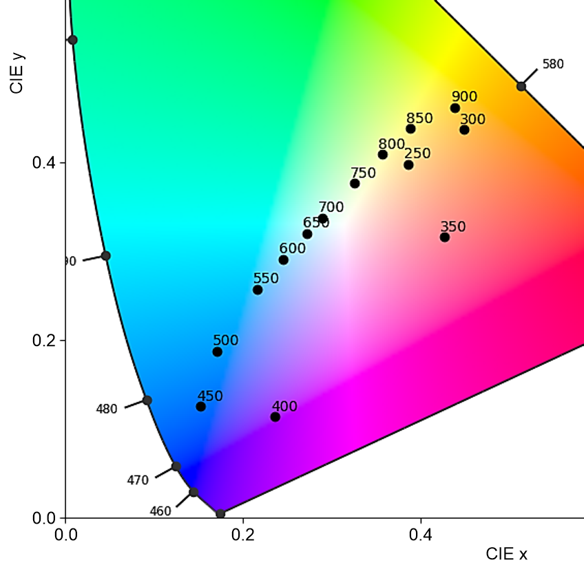
Fig. 6. The influence of the number of ALD cycles on the colour of the ZnO thin film deposited on a silicon substrate showing in the CIE colour space.
yellow axis (b*) – which is especially useful for identifying subtle differences in the visual appearance of the deposited ZnO layers. By offering a perceptually uniform colour space, the CIE Lab model ensures that any observed changes in the coatings, whether due to differences in thickness, material composition, or ALD cycle parameters, can be described in a way that aligns with human visual perception. Consequently, the use of the CIE Lab colour space in this work significantly amplifies the accuracy and relevance of the colour analysis, providing valuable insights into the optical characteristics influenced by the advanced deposition techniques.
The coloration of the ZnO-coated silicon substrates arises from thin-film interference effects that occur when light is reflected multiple times at the air/ZnO and ZnO/Si interfaces. Due to the finite thickness and relatively high refractive index of wurtzite ZnO, partial reflections at these interfaces generate phase-shifted light waves that interfere either constructively or destructively, depending on the optical path length within the film. As the ZnO thickness increases with the number of ALD cycles, the interference condition shifts across the visible spectrum, selectively enhancing specific wavelength ranges while suppressing others. This results in the observed sequence of interference colours, such as blue, violet, gold, and green. The perceived colour is therefore determined not only by film thickness but also by the refractive index of ZnO and the optical properties of the silicon substrate, which acts as a reflective back surface. Since ALD enables precise thickness control and yields films with consistent optical constants, interference-driven colouration provides a reliable, reproducible optical indicator of ZnO layer thickness.
It should be emphasised that the interference colours of ZnO layers are strongly dependent on the optical properties of the underlying substrate. In addition, the investigation of ZnO layers deposited on plain silicon wafers served as a reference system, allowing us to systematically evaluate the thickness-dependent optical behaviour of ZnO under well-defined, reproducible conditions. This reference analysis enabled calibration of the ALD process and identification of thickness–colour relationships independent of device- specific effects. Based on this understanding, the deposition process was subsequently transferred to silicon PV devices, where the same thickness control was applied to intentionally reproduce targeted interference colours on a more complex, optically known substrate. The observed colour differences, therefore, reflect the substrate-dependent optical response rather than inconsistencies in the deposition process.
The colorimetric analysis shown in Fig. 6 was performed on ZnO films deposited on mirror-polished, planar silicon wafers, which serve as optically uniform, highly reflective substrates. In contrast, the PV devices shown in Fig. 7 comprise multilayer stacks, including surface texturing, passivation coatings, anti-reflective layers, and metallic front contacts. These additional layers modify the effective refractive index contrast and phase conditions at the interfaces, leading to a shift in the interference maxima and, consequently, to different perceived colours for ZnO films of identical thickness. Furthermore, the macroscopic texture of the solar cell surface and variations in illumination and viewing geometry during image acquisition contribute to differences in colour appearance. As a result, direct visual colour comparison between ZnO-coated silicon wafers and ZnO-coated PV devices should be interpreted qualitatively rather than as an exact thickness–colour correspondence.
Following the initial evaluation of film thickness and optical appearance, the ALD process was repeated on three monocrystalline silicon solar cells. Depositions were performed using 500, 700, and 900 cycles, leading to a progressive colour shift – from navy blue to gold, purple, and ultimately green (Fig. 7). The electrical performance of the modified silicon PV cells was assessed using a solar simulator, with the corresponding parameters summarised in Table 4.
The effect of increasing the ZnO layer thickness on the PV performance of solar cells was analysed by systematically varying the thickness of three identical devices. Initially, all uncoated samples (1, 2, and 3) exhibited a characteristic deep navy-blue colour, confirming their comparable initial state and optical properties. After baseline measurements, each of these samples was sequentially coated with increasingly thick ZnO films, resulting in distinct interference colours: golden for the thinnest layer (1+ZnO), violet for the intermediate layer (2+ZnO), and green for the thickest one (3+ZnO). These colour changes correlate with increasing film thickness, offering a visual indication of the ZnO growth. A clear decline in the opencircuit voltage (V OC) was observed with the introduction and subsequent thickening of the ZnO layer. While the initial V OC for the uncoated samples was consistent at approximately 0.632 V, it dropped to 0.621 V, 0.620 V, and 0.619 V for the golden, violet, and green samples, respectively. This systematic reduction suggests that thicker ZnO layers may introduce additional recombination centres or interfacial barriers, thereby impairing carrier separation.
Although ZnO is generally regarded as a wide-bandgap and highly transparent oxide in the visible spectral range, its optical absorption cannot be considered negligible when the film thickness increases to several tens or hundreds of nanometers. In particular, ZnO exhibits increased absorption in the near-ultraviolet and blue regions of the spectrum, where silicon solar cells still possess a non-zero spectral response. As the ZnO layer becomes thicker,
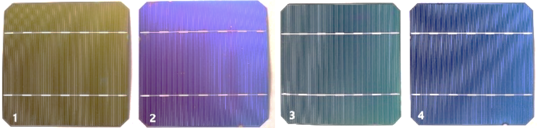
Fig. 7. Optical photographs of monocrystalline silicon solar cells: (1) cell coated with a ZnO layer deposited using 500 ALD cycles (golden appearance), (2) cell coated with a ZnO layer deposited using 700 ALD cycles (violet appearance), (3) cell coated with a ZnO layer deposited using 900 ALD cycles (green appearance), and (4) uncoated reference silicon solar cell (navy-blue appearance). The images illustrate the thickness-dependent interference colours of the ZnO coatings.
Summary of the PV performance metrics of the solar cells before and after undergoing the ALD procedure.
| Parameters | Solar devices
before modification |
Solar devices
after modification |
||||
|---|---|---|---|---|---|---|
| 1 | 2 | 3 | 1+ZnO | 2+ZnO | 3+ZnO | |
| VOC [V] | 0.632 | 0.633 | 0.632 | 0.621 | 0.620 | 0.619 |
| ISC [A] | 5.610 | 5.625 | 5.670 | 5.295 | 5.245 | 5.310 |
| VMPP [V] | 0.474 | 0.472 | 0.470 | 0.466 | 0.467 | 0.469 |
| IMPP [A] | 5.015 | 4.980 | 5.040 | 4.513 | 4.475 | 4.482 |
| MPP [W] | 2.377 | 2.351 | 2.369 | 2.105 | 2.091 | 2.102 |
| FF | 0.669 | 0.658 | 0.658 | 0.640 | 0.643 | 0.641 |
| η [%] | 15.26 | 15.10 | 15.21 | 13.52 | 13.43 | 13.50 |
parasitic absorption within the coating may reduce the photon flux reaching the silicon absorber, thereby lowering the short-circuit current and overall conversion efficiency. This effect may partially explain the monotonic decrease in PV performance observed for increasing ZnO thickness. Furthermore, thickness-induced interference effects can modify the effective optical path and local field intensity within the ZnO layer, potentially amplifying absorption losses in the thickest films. These considerations highlight the importance of carefully balancing ZnO thickness to minimise optical absorption while preserving potential benefits such as surface passivation and anti-reflective behaviour.
Similarly, the short-circuit current (ISC) decreased from an average of ~ 5.6 A in the uncoated cells to values ranging between 5.245 A and 5.310 A in the ZnO-coated counterparts. This trend indicates a growing limitation in light absorption or carrier collection efficiency, possibly due to increased reflection or sub-bandgap absorption within the ZnO layer, especially at higher thicknesses. Maximum power point parameters (VMPP, IMPP) and the overall maximum output power (MPP) also declined with increasing ZnO thickness. The output power dropped from approximately 2.37 W in the uncoated samples to around 2.10 W in the thickest ZnO-coated device. Correspondingly, the fill factor (FF) decreased from ~ 0.66 to ~ 0.64, highlighting potential increases in series resistance or a deterioration in charge extraction efficiency introduced by the ZnO overlayer. The overall energy conversion efficiency (η) dropped from an average of 15.2% in the uncoated samples to approximately 13.5% for the thickest ZnO-coated sample. Although the efficiency decrease was consistent with increasing ZnO thickness, a subtle recovery in performance was observed in the green (thickest) sample relative to the violet one. This may suggest a trade-off between optical losses and surface passivation, where beyond a certain thickness, the ZnO layer begins to contribute positively by reducing surface recombination.
The partial recovery of PV performance observed for the thickest ZnO-coated sample suggests that, beyond a certain thickness, the ZnO layer may begin to play a more complex functional role than merely introducing optical and electrical losses. One contributing factor may be improved surface passivation at the ZnO/Si interface, which can reduce surface recombination by saturating dangling bonds and mitigating defect-related carrier losses. Additionally, thickness-dependent optical interference effects may alter the device spectral reflectance, enhancing light coupling into the silicon absorber at selected wavelengths. Another potential mechanism, though not directly investigated in this study, involves the intrinsic photoluminescence of ZnO, which is known to absorb ultraviolet radiation and reemit it in the near-visible range. Such down-conversion could, in principle, increase the fraction of incident photons within the spectral response range of silicon. While the present results do not allow a definitive separation of these effects, the observed trend suggests that an optimal ZnO thickness exists at which the beneficial effects of surface passivation and optical modification begin to compensate for thickness-related losses.
The ZnO thickness range applied to the PV devices (approximately 90–160 nm, corresponding to 500–900 ALD cycles) was selected to ensure fully continuous films while avoiding the early nucleation regime and excessive optical losses. Within this intermediate thickness window, the observed variations in PV efficiency are relatively small, indicating that the dominant performance reduction arises from the introduction of the ZnO overlayer itself rather than from thickness alone. Thickness-dependent effects – such as interference-related spectral redistribution, increasing parasitic absorption, and gradual modification of interfacial recombination – contribute as secondary mechanisms and manifest as systematic but moderate trends. Thinner ZnO layers do not provide stable or reproducible optical behaviour, whereas significantly thicker coatings are expected to further reduce efficiency due to enhanced absorption and increased series resistance. These results suggest that ZnO thickness primarily modulates device performance once a continuous layer is formed, rather than acting as the sole determining factor.
In conclusion, while the deposition of ZnO layers on the surface of solar devices systematically alters their optical appearance and electrical performance, the relationship is clearly thickness-dependent. Thinner ZnO coatings lead to decreased performance due to optical and electrical losses, but an optimal thickness range may exist in which the benefits of surface passivation and anti-reflective effects begin to outweigh the drawbacks. These findings emphasise the need to carefully optimise ZnO thickness when used as a functional coating in PV devices.
4. Conclusions
This study systematically investigated the influence of ALD-deposited ZnO thin films on the optical properties and electrical performance of silicon PV cells. By varying the number of ALD cycles, precise control over the ZnO film thickness was achieved, enabling reproducible tuning of interference-related colouration across a broad visible spectrum. The combined RGB and CIE Lab colour space analyses confirmed that the observed colour evolution correlates consistently with film thickness and aligns well with human visual perception, demonstrating the effectiveness of ALD as a tool for controlled optical surface engineering.
A reference analysis performed on planar, mirrorpolished silicon substrates isolated the intrinsic thicknessdependent optical behaviour of ZnO under well-defined boundary conditions. This reference framework enabled subsequent transfer of the deposition process onto silicon PV devices, where the same thickness control was used to intentionally reproduce selected interference colours on a more optically complex substrate. Differences in perceived colour between planar silicon and PV devices were shown to arise from substrate-dependent interference conditions rather than from variations in ZnO growth or deposition parameters.
From an electrical standpoint, the introduction of the ZnO overlayer led to a systematic reduction in PV performance, including decreases in energy conversion efficiency (η), short-circuit current (ISC), open-circuit voltage (VOC), and fill factor (FF). The average efficiency decreased from approximately 15.2% for uncoated cells to about 13.5% for the thickest ZnO-coated devices. These losses are primarily attributed to additional optical reflection and parasitic absorption in the ZnO layer, as well as to interfacial effects that may enhance carrier recombination and series resistance. Within the investigated thickness range (approximately 90–160 nm), the observed efficiency variations were moderate, indicating that the dominant impact arises from the presence of the ZnO layer itself, while thickness-dependent effects act as secondary modulation mechanisms.
Notably, a subtle stabilisation or partial recovery of performance at the highest investigated thickness suggests the presence of competing effects, such as improved surface passivation, interference-induced spectral redistribution, or changes in interfacial recombination dynamics. This observation implies that an optimal ZnO thickness window may exist in which the optical and electrical trade-offs are partially balanced, although identifying this optimum requires further targeted investigation.
Overall, the results demonstrate that ALD-deposited ZnO thin films can serve a dual function in PV systems: as functional coatings that modify optical and electrical behaviour and an effective means of tailoring the visual appearance of PV devices. This duality offers promising opportunities for the aesthetic integration of solar modules into architecturally sensitive environments, where visual design is a key consideration. Future work should focus on optimising ZnO thickness, interface engineering, and layer composition, as well as on extending optical characterisation and device-level analysis to achieve a better balance between aesthetic customisation and PV performance.
Authors’ statement
Research concept and design, M.S.; collection and/or assembly of data, M.S., M.M.S.; data analysis and interpretation, M.S., M.M.S., J.P.; writing the article, M.S., M.M.S.; critical revision of the article, M.S., K.M., J.P.; final approval of the article, M.S.
Acknowledgements
Publication supported as part of the Excellence Initiative – Research University program implemented at the Silesian University of Technology, 2025.
References
[1] Green, M. A. et al. Solar cell efficiency tables (Version 58). Prog. Photovolt. 29, 657–667 (2021). https://doi.org/10.1002/pip.3444
[2] Zhou, J. et al. Recent advancements in poly-Si/SiOx passivating contacts for high-efficiency silicon solar cells: Technology review and perspectives. J. Mater. Chem. A 10, 20147–20173 (2022). https://doi.org/10.1039/D2TA04730F
[3] Wu, Y. N., Zhang, T., Gao, R. & Wu, C. Portfolio planning of renewable energy with energy storage technologies for different applications from electricity grid. Appl. Energy 287, 116562 (2021). https://doi.org/10.1016/j.apenergy.2021.116562
[4] Yin, S. & Wang, J. State-of-the-art short-term electricity market operation with solar generation: A review. Renew. Sustain. Energy Rev. 138, 110647 (2021). https://doi.org/10.1016/j.rser.2020.110647
[5] Drygala, A. et al. Influence of laser texturization surface and atomic layer deposition on optical properties of polycrystalline silicon. Int. J. Hydrog. Energy 41, 7563–7567 (2016). https://doi.org/10.1016/j.ijhydene.2015.12.180
[6] Drabczyk, K., Kulesza-Matlak. G., Drygala, A., Szindler. M. & Lipiński, M. Electroluminescence imaging for determining the influence of metallization parameters for solar cell metal contacts. Sol. Energy, 126, 14–21 (2016). - https://doi.org/10.1016/j.solener.2015.12.029
[7] Marszalek, M., Winkowski, P. & Jaglarz, J. Optical properties of the Al2O3/SiO2 and Al2O3/HfO2/SiO2 antireflective coatings. Mater. Sci.-Pol. 32, 80–87 (2014). https://doi.org/10.2478/s13536-013-0156-y
[8] Wojtasik, K. et al. Zinc oxide films fabricated via sol-gel method and dip-coating technique–effect of sol aging on optical properties, morphology, and photocatalytic activity. Materials 16, 1898 (2023). https://doi.org/10.3390/ma16051898
[9] Malpure, N. N. et al. Influence of multilayer architecture on the structural, optical, and photoluminescence properties of ZnO thin films. Photonics 12, 1219 (2025). https://doi.org/10.3390/photonics12121219
[10] Sandeep, K. M., Shreesha, B. & Dharmaprakash, S. M. Structural, optical, and LED characteristics of ZnO and Al-doped ZnO thin films. J. Phys. Chem. Solids 104, 36–44 (2017). https://doi.org/10.1016/j.jpcs.2017.01.003
[11] Lee, J. H., Choi, M. J, Kang, S. M, Eum, H. I. & Kim, G. H. Structural color formation of ZnO nanorods using gold as a seed and reflective layer. ACS Appl. Nano Mater. 7, 8655–8660 (2024). https://doi.org/10.1021/acsanm.3c06170
[12] George, S. M. Atomic layer deposition: An overview. Chem. Rev. 110, 111–131 (2010). https://doi.org/10.1021/cr900056b
[13] Iqbal, J. et al. ALD grown nanostructured ZnO thin films: Effect of substrate temperature on thickness and energy band gap. J. King Saud Univ. Sci. 28, 347–354 (2016). https://doi.org/10.1016/j.jksus.2016.03.001
[14] Fei, Y. et al. Properties study of ZnO films prepared by ALD. J. Mol. Struct. 1269, 133804 (2022). https://doi.org/10.1016/j.molstruc.2022.133804
[15] Sahayaraj, S. et al. Tuning the optical and electrical properties of ALD-grown ZnO films by germanium doping. Materials 17, 2906 (2024). https://doi.org/10.3390/ma17122906
[16] Mousa, M. B. M, Oldham, C. J., Jur, J. S. & Parsons, G. N. Effect of temperature and gas velocity on growth per cycle during Al2O3 and ZnO atomic layer deposition at atmospheric pressure. J. Vac. Sci. Technol. A: Vac. Surf. Films 30, 01A155 (2012). https://doi.org/10.1116/1.3670961
[17] Perrotta, A., Pilz, J., Resel, R., Werzer, O. & Coclite, A. M. Initial growth and crystallization onset of plasma enhanced-atomic layer deposited ZnO. Crystals 10, 291 (2020). https://doi.org/10.3390/cryst10040291
[18] Tapily, K., Gu, D. & Baumgart, H. Growth mechanism of ALD ZnO films investigated by physical characterization. ECS Trans. 33, 355–362 (2010). https://doi.org/10.1149/1.3485271
[19] Domanowska, A. et al. Sol-gel derived SiOx:TiOy films for integrated optics: HR S/TEM and AES/XPS insight to structure and chemical composition. Mater. Sci. Eng. B 303, 117289 (2024). https://doi.org/10.1016/j.mseb.2024.117289
[20] Mousa, H. M., Shabat, M. M. & Karmoot, M. R. Double layer antireflection coating design for conductive solar cells. Rom. Rep. Phys. 72, 416 (2020). https://rrp.nipne.ro/2020/AN72416.pdf
[21] Soman, A. & Antony, A. Colored solar cells with spectrally selective photonic crystal reflectors for application in building integrated photovoltaics. Sol. Energy 188, 1–8 (2019). http://doi.org/10.1016/j.solener.2019.01.058
[22] Seo, J.-W., Choi, S.-W., Kim, Y., Kwon, S.-H. & Kwon, J.-D. Surface modification of color-clarifying layer in transparent conductive oxide based distributed Bragg reflector-diffuser electrode for building-integrated photovoltaics. Sol. Energy 263, 111924 (2023). https://doi.org/10.1016/j.solener.2023.111924
[23] Zhou, Y. et al. Energy-efficient colorful silicon photovoltaic modules driven by transparent-colored radiative cooling. Sol. Energy Mater. Sol. Cells 259, 112459 (2023). https://doi.org/10.1016/j.solmat.2023.112459
[24] Boryło, P. et al. The influence of atomic layer deposition process temperature on ZnO thin film structure. Appl. Surf. Sci. 474, 177– 186 (2019). https://doi.org/10.1016/j.apsusc.2018.03.169
[25] Cuscó, R. et al. Temperature dependence of Raman scattering in ZnO. Phys. Rev. B 75, 165202 (2007). https://doi.org/10.1103/PhysRevB.75.165202
[26] Thangavel, R. et al. Cesium doped and undoped ZnO nanocrystalline thin films: A comparative study of structural and micro-Raman investigation of optical phonons. J. Raman Spectrosc. 41, 1594–1600 (2010). https://doi.org/10.1002/jrs.2599
[27] Jothilakshmi, R. et al. Micro-Raman scattering spectroscopy study of Li-doped and undoped ZnO needle crystals. J. Raman Spectrosc. 40, 556–561 (2009). https://doi.org/10.1002/jrs.2164